Method of attaching layer material and forming layer in predetermined pattern on substrate using mask

a technology of predetermined pattern and layer material, which is applied in the direction of identification means, instruments, vacuum evaporation coating, etc., can solve the problems of high precision, anodes, organic materials, other components formed on glass substrates, etc., and achieve high precision

Inactive Publication Date: 2002-06-20
SANYO ELECTRIC CO LTD
View PDF8 Cites 169 Cited by
  • Summary
  • Abstract
  • Description
  • Claims
  • Application Information

AI Technical Summary

Benefits of technology

[0019] The present invention has been conceived in view of the above-described problems, and aims to provide a method of attaching a layer material, such as an emissive material, onto a predetermined position of a substrate with a high precision to form a layer in a desired pattern without generating a scar with a mask and the like.
[0021] According to another aspect, the present invention provides a method of forming an individually patterned layer in a plurality of regions of a substrate, comprising the step of disposing between the substrate and a layer material source a mask having a smaller area than the substrate and including an opening corresponding to one or more of the plurality of regions where the layer is formed, and the step of causing relative movement between the mask and the layer material source, and the substrate, and causing a material scattered from the layer material source to attach onto the substrate through the opening, thereby forming the individually patterned layer.
[0027] By thus causing evaporation of a material in a material source while shifting a relative position between the material source and the mask, and the substrate, a material layer can be formed on the substrate through the opening formed in the mask with high positional and patterning accuracies. Because a mask having a smaller area than the substrate is employed as described above, the mask can be provided with a high strength and the opening formed with a high accuracy, and variation in distance between the material source and the respective positions of the mask can be reduced, making it possible to form the material layer at a plurality of positions of the substrate with a very high accuracy and balanced characteristics.
[0032] As described above, the method according to the present invention allows formation of the individually patterned material layer at predetermined positions of the substrate as desired with a high accuracy. Consequently, emissive material layers for different colors, for example, can be formed with a high accuracy, so that color emissive devices and display devices presenting vivid and uniform colors can be manufactured.
[0034] Use of a semiconductor material for the mask enables formation of the opening by photolithography with a high accuracy and a sufficient strength to be maintained, thereby contributing to improvement in accuracy of patterning the material layer to be formed, and facilitating handling of the mask to, for example, increase life of the mask, so that the cost of manufacturing a device using such a mask can be reduced.
[0037] Thus, when the emissive material layer is formed in individual patterns for the respective pixel regions, the opening corresponding to the individual pattern is formed in the mask, and the material is attached to the substrate while the emissive material source and the substrate are moved relatively. Consequently, the emissive material source is located equally close to each region for forming the emissive material layer on the substrate, thereby preventing variation in thickness of the emissive material layer formed in each of such regions caused by shadowing.

Problems solved by technology

When a single, large-sized metal mask is thus used, it becomes extremely difficult to form a mask with a high precision as the size of the mask increases, and shadowing, i.e. blocking the evaporated material scattered from the source by the edges of the mask in the openings, also becomes more prominent in the peripheral region of the glass substrate 10.
However, when the mask is brought into contact with the substrate, the anodes, the organic material, and other components formed on the glass substrate may be damaged by the mask.

Method used


Image

  • Method of attaching layer material and forming layer in predetermined pattern on substrate using mask
  • Method of attaching layer material and forming layer in predetermined pattern on substrate using mask
  • Method of attaching layer material and forming layer in predetermined pattern on substrate using mask

Examples


second embodiment

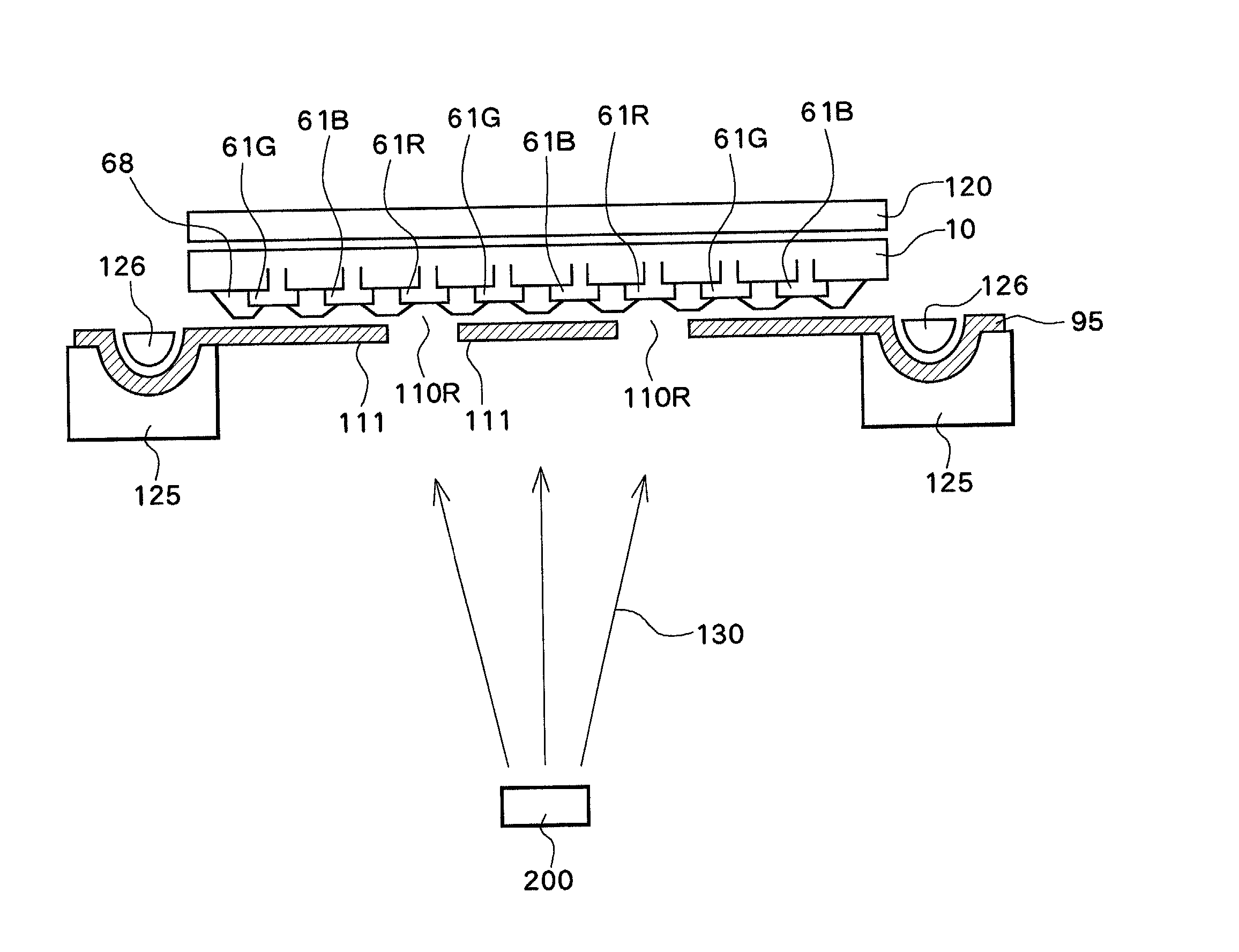
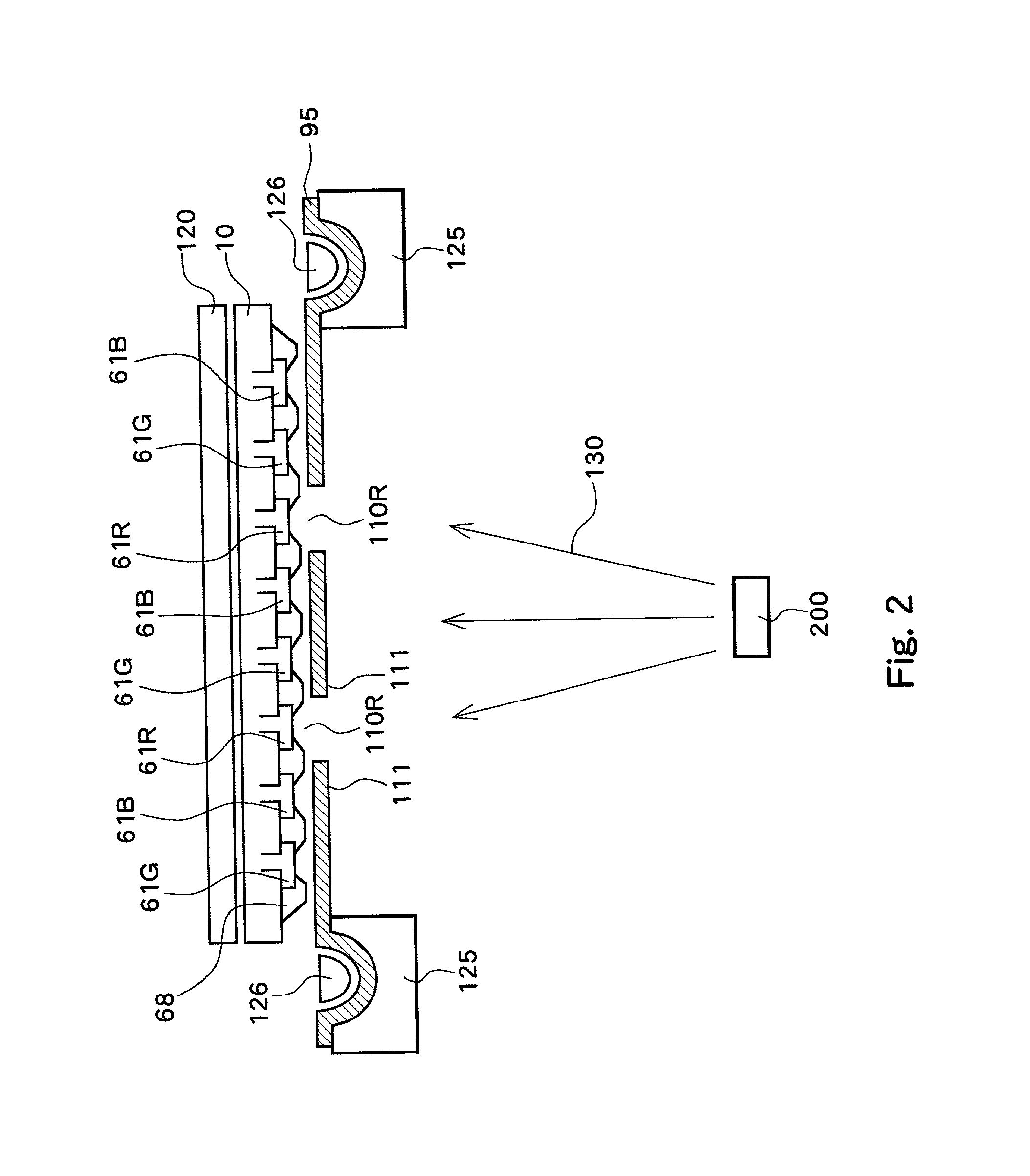
[0096] As described above, according to the present invention, the evaporation mask 100 smaller in size than the substrate 10 is employed to evaporate the organic material for the identical color onto the substrate 10 a plurality of times. Further, the linearly extending source 210 extending in the direction in which the evaporation mask 100 is provided is employed. As a result, variation in evaporating conditions for the respective openings 110 is reduced, thereby preventing variation in thickness of the evaporation layer. Consequently, problems, such as variation in tone of the same color between the central portion and the peripheral portion of the glass substrate 10, can be avoided, and the organic material to be evaporated onto a given anode is prevented from reaching and being attached onto the adjacent anodes for different color pixel regions, thereby preventing blurring caused by color mixture.

[0097] Further, flexure of the evaporation mask 100 according to the second embodi...

first embodiment

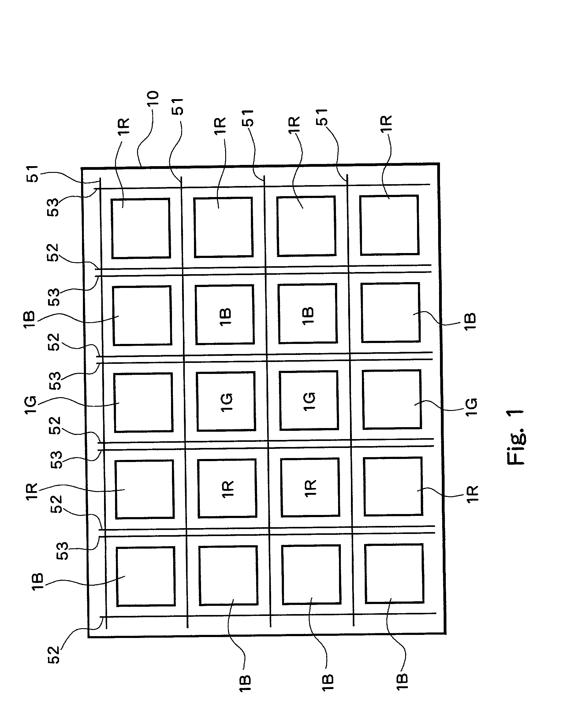
[0099] Further, while in the above-described first embodiment the single large substrate 10 is divided into four evaporation regions as shown in FIG. 3, naturally the number by which the substrate is divided is not limited to four in the present invention. However, because the insulating substrate is slid in vertical and horizontal directions of FIG. 3 (X and Y directions, respectively) for evaporation, this number is preferably an even number in light of the evaporation process efficiency.

[0100] While the display pixels for the respective colors are described as being arranged as stripes in the above embodiments, other arrangements are also possible, and the present invention can also be applied to a display device having display pixels in the so-called delta arrangement or in a variety of other arrangements. In such a case, the present invention can be readily implemented by using an evaporation mask having openings corresponding to the arrangement of the respective color display ...


PUM

PropertyMeasurementUnit
thicknessaaaaaaaaaa
thicknessaaaaaaaaaa
thicknessaaaaaaaaaa

Abstract

Upon formation of a layer such as an emissive layer of an organic EL element by attaching an emissive material onto a substrate (10), an evaporation mask (100) including an opening (110) corresponding to the layer formed to have a plurality of individual patterns and having an area, for example, smaller than the substrate is disposed between the substrate (10) and a material source (200). A relative position between the mask (100) and the material source (200), and the substrate (10) is slid by a predetermined pitch corresponding to the size of a pixel of the substrate (10), thereby forming a material layer (such as the emissive layer 64) in a predetermined region of the substrate. As a result, the material layer can be formed on the substrate through, for example, evaporation with a high accuracy.

Description

[0001] 1. Field of the Invention[0002] The present invention relates to a color display device employing an electroluminescent (hereinafter referred to as "EL") element as an emissive element, and a method of manufacturing such a color display device.[0003] 2. Description of the Related Art[0004] In recent years, EL display devices comprising EL elements have gained attention as potential replacements for CRTs and LCDs.[0005] Research has been directed to the development of active matrix EL display devices comprising a thin film transistor (hereinafter referred to as a "TFT") as a switching element for driving the EL element.[0006] FIG. 1 is a diagram illustrating an arrangement of display pixels 1R, 1G, and 1B for respective colors in a color organic EL display device.[0007] As shown in the figure, the active matrix organic EL display device includes the display pixels 1R, 1G, and 1B for red (R), green (G), and blue (B), respectively, which are formed in regions on a substrate 10 s...

Claims


Application Information

Patent Timeline
Patent Type & Authority Applications(United States)
IPC IPC(8): C23C14/04H05B33/10G09F9/00G09F9/30H01L27/32H01L51/00H01L51/30H01L51/40H01L51/50H01L51/56H05B33/12
CPCC23C14/042H01L27/3211H01L51/001H01L51/0011H01L51/56H01L51/0059H01L51/0062H01L51/0081H01L51/0013H10K59/35H10K71/18H10K71/164H10K71/166H10K85/649H10K85/631H10K85/324H10K71/00H05B33/10
Inventor YAMADA, TSUTOMUYONEDA, KIYOSHI
Owner SANYO ELECTRIC CO LTD
Why Eureka
Try Eureka