Semiconductor device, manufacturing method thereof, and electronic apparatus

Inactive Publication Date: 2002-08-15
SEIKO EPSON CORP
View PDF5 Cites 0 Cited by
  • Summary
  • Abstract
  • Description
  • Claims
  • Application Information

AI Technical Summary

Benefits of technology

[0005] Specifically, it is expected that forming elements, each having the photogate integrated with the MOS transistor, allows the considerable leakage current to be lowered and prevents the electric charge caused by the high-energy incident light from intruding into the photogate, in the SOI substrate or the like.
[0008] By forming the elements, each having a photogate integrated with a MOS transistor, in a semiconductive layer which is deposited on an insulating layer to form a substrate, such as an SOI, junction leakage current flowing between the source or the drain of the MOS transistor and the semiconductive layer is reduced, and consequently the S / N ratio and the dynamic range can be improved.
[0009] Also, by forming the semiconductor device in a semiconductive layer which is deposited on an insulating layer to form a substrate, electric charge generated by light is prevented from deeply penetrating the semiconductive layer, and consequently the electric charge can be efficiently collected.
[0011] Thus, the phototransformation efficiency of the photogate and the switching-speed performance of the MOS transistor are effectively improved.
[0014] By forming the semiconductor device such that the semiconductive layer forming the photogate comes into contact with the source area of the MOS transistor, the electric charge converted by the photogate is quickly transferred to the source area of the MOS transistor, and thus the electric charge can be efficiently transferred.
[0017] The method of manufacturing a semiconductor device includes the step of preparing an SOI substrate formed by depositing a silicon layer on an insulating layer, and the elements, each having a photogate integrated with a MOS transistor. As a result, semiconductor devices capable of effectively avoiding problems caused by forming elements on a bulk silicon substrate can be manufactured.

Problems solved by technology

In the case of an integrated circuit (IC) or a large-scale integration (LSI) circuit, transistors are densely integrated to highly integrate semiconductor elements; however, the elements directly formed in the bulk silicon substrate allow considerable junction leakage current to occur between a silicon layer and a source connected to the output circuit or between the silicon layer and a drain.
The leakage current acts as dark current which causes noise, thereby lowering the S / N ratio and the dynamic range.

Method used


Image

  • Semiconductor device, manufacturing method thereof, and electronic apparatus
  • Semiconductor device, manufacturing method thereof, and electronic apparatus
  • Semiconductor device, manufacturing method thereof, and electronic apparatus

Examples


Embodiment Construction

[0028] An embodiment of the present invention will now be described with reference to drawings. FIGS. 1 to 7 are fragmentary sectional views showing part of the manufacturing process of a semiconductor device according to the embodiment of the present invention.

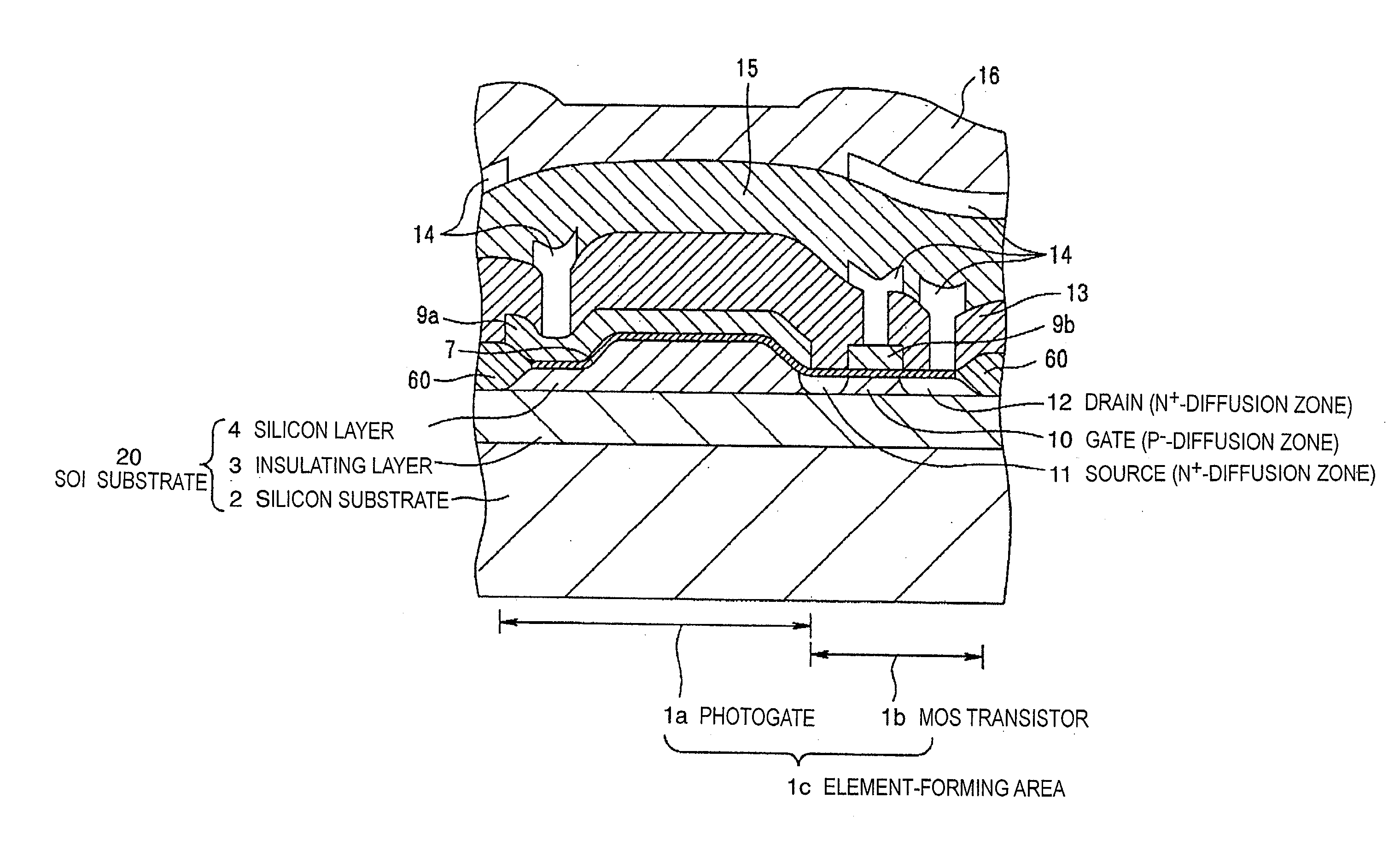
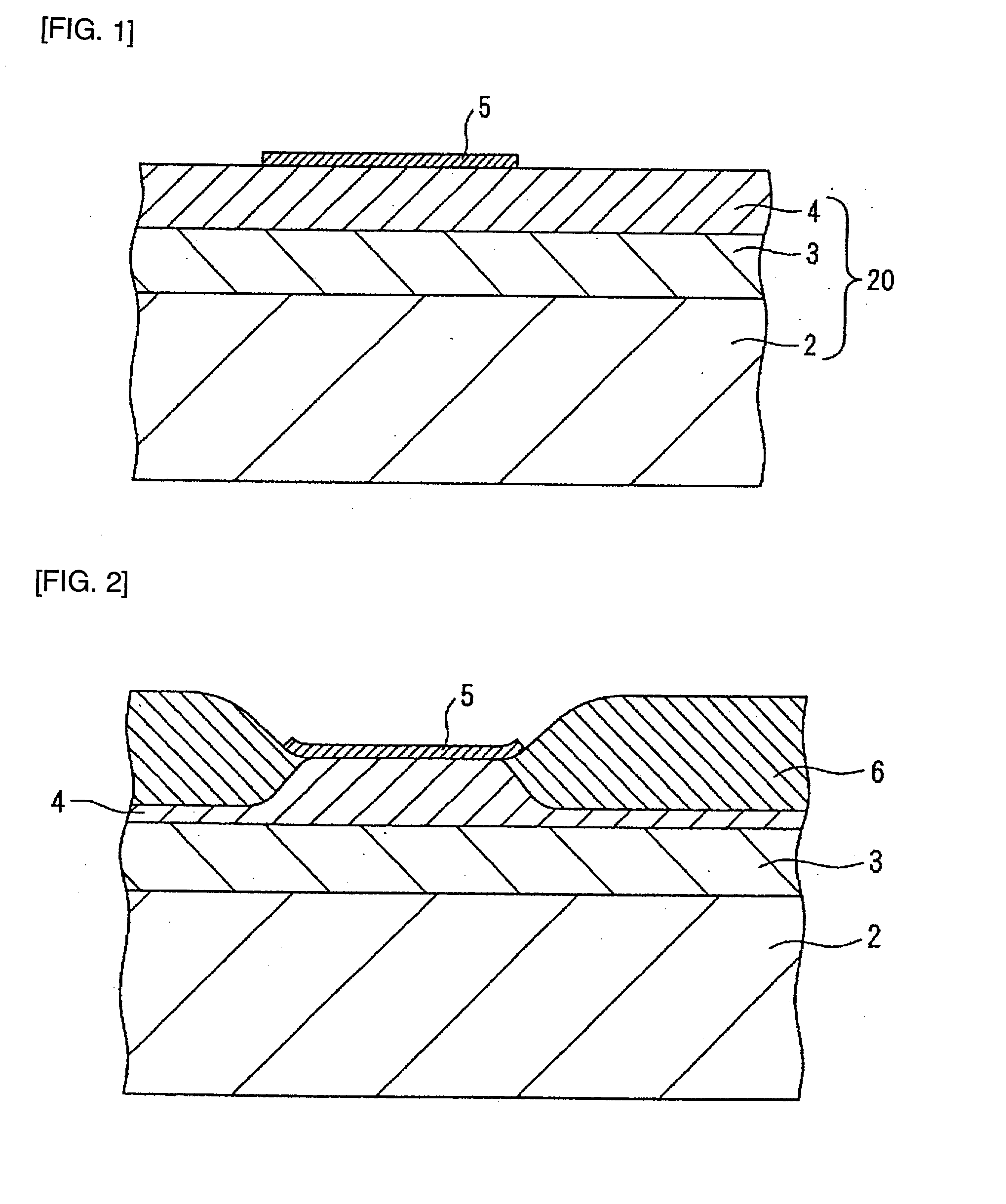
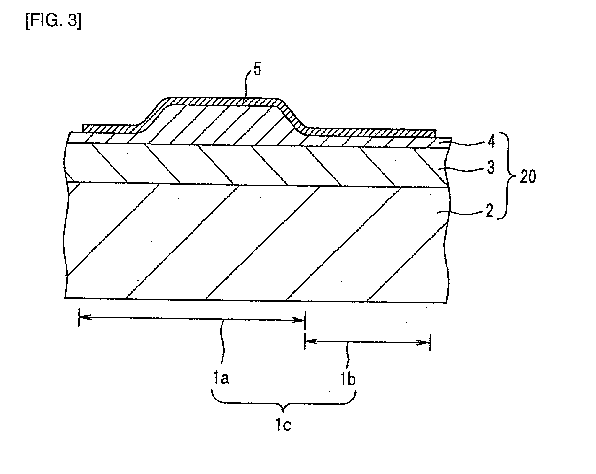
[0029] First, a completed semiconductor device 1 will be briefly described. As shown in FIG. 7, the semiconductor device 1 is formed in an SOI substrate 20 formed by depositing an insulating layer 3 formed of silicon oxide and a thin silicon layer 4 on a thick p-type silicon substrate 2 in that order. The silicon layer 4 can serve as a photogate 1a for converting absorbed light into an electric charge and a MOS transistor 1b for transferring the electric charge. The area of the silicon layer 4 serving as the photogate 1a has a thickness larger than that of the area of the silicon layer 4 serving as the MOS transistor 1b.

[0030] The silicon layer 4 is covered with a gate oxide 7. Gate electrodes 9a and 9b are formed of polycrys...


PUM


Abstract

A semiconductor device, a manufacturing method, and an electronic apparatus are provided. The semiconductor device comprises elements, each having a photogate for converting light into an electric charge integrated with a MOS transistor for transferring the electric charge, formed in a substrate formed by depositing a semiconductive layer on an insulating layer. The elements, each having the photogate integrated with the MOS transistor, are formed in an SOI substrate formed by depositing a silicon layer on an insulating layer. The thickness of the silicon layer forming the photogate for converting light into an electric charge is larger than that of the silicon layer forming the MOS transistor for transferring the electric charge. Also, the integrated elements are arranged in a matrix manner.

Description

[0001] The present invention relates to semiconductor devices and methods of manufacturing the same. In particular, the present invention relates to a semiconductor device comprising elements, each having a photogate for converting light into an electric charge integrated with a transistor for transferring the electric charge. The elements are formed in a semiconductive layer which is deposited on an insulating layer to form a substrate, such as an SOI substrate, which is formed by depositing a silicon layer on an insulating layer. The present invention also relates to a method of manufacturing the semiconductor device and electronic apparatuses.[0002] Elements, each having a structure in which a photogate and a MOS transistor are integrated with each other, have been recently used as a semiconductor device for transferring light as electrical signals. These elements are integrated on a bulk silicon substrate to form a semiconductor device in which the photogate converts absorbed li...

Claims


Application Information

Patent Timeline
IPC IPC(8): H01L21/00H01L27/146H01L27/148H01L29/768H01L29/786H01L31/062H01L31/10H01L31/113H04N5/335H04N5/361H04N5/369
CPCH01L27/14601
Inventor IRIGUCHI, CHIHARU
Owner SEIKO EPSON CORP
Why Eureka
Try Eureka