Method for producing an image display apparatus
a technology of image display and apparatus, which is applied in the direction of vacuum obtaining/maintenance, electric discharge tube/lamp manufacturing, discharge tube luminescnet screen, etc., can solve the problems of deterioration of electron source, destruction of apparatus, and inability to display bright images
- Summary
- Abstract
- Description
- Claims
- Application Information
AI Technical Summary
Benefits of technology
Problems solved by technology
Method used
Image

Examples
first embodiment
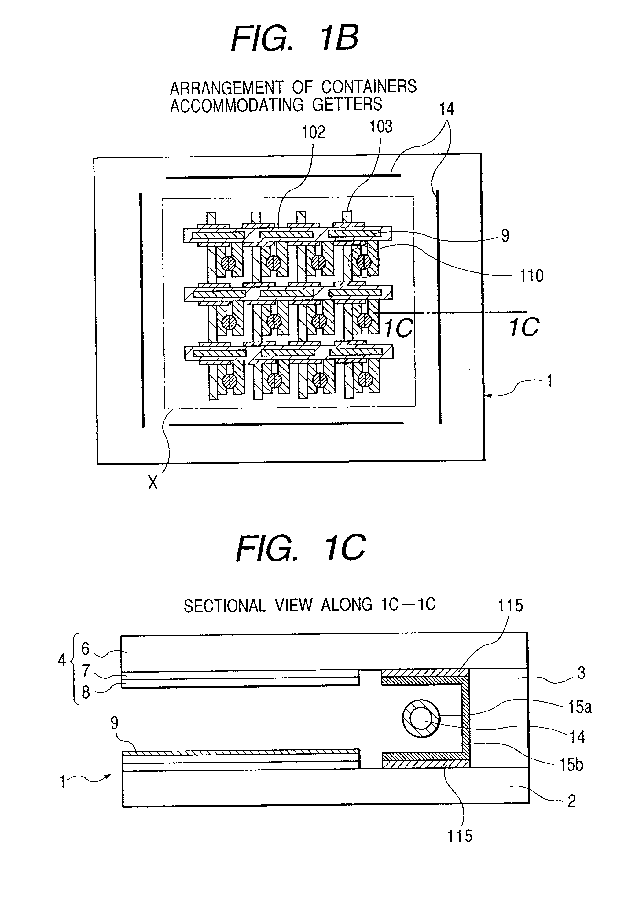
[0188] In this reference example, an image display apparatus was prepared in the same manner as in the first embodiment, except that an evaporating getter was positioned on only one side outside the image display area.
[0189] In this reference example, the evaporating getter 14 was provided on one side outside the image display area as shown in FIGS. 20A and 20B, and the getter film was formed by flushing the evaporating getter 14 with a heating wire 15 after the sealing.
[0190] Each of the image display apparatus of the foregoing embodiments first to fifth and the reference example was subjected to simple matrix drive to effect continuous light emission over the entire surface and the luminance variation in time was measured.
[0191] As a result, though there was difference in the initial luminance, the image display apparatus of the embodiments first to fifth showed scarce decrease of the luminance and scarce fluctuation in the luminance among the pixels even after a prolonged drive, ...
sixth embodiment
[0192] [Sixth Embodiment]
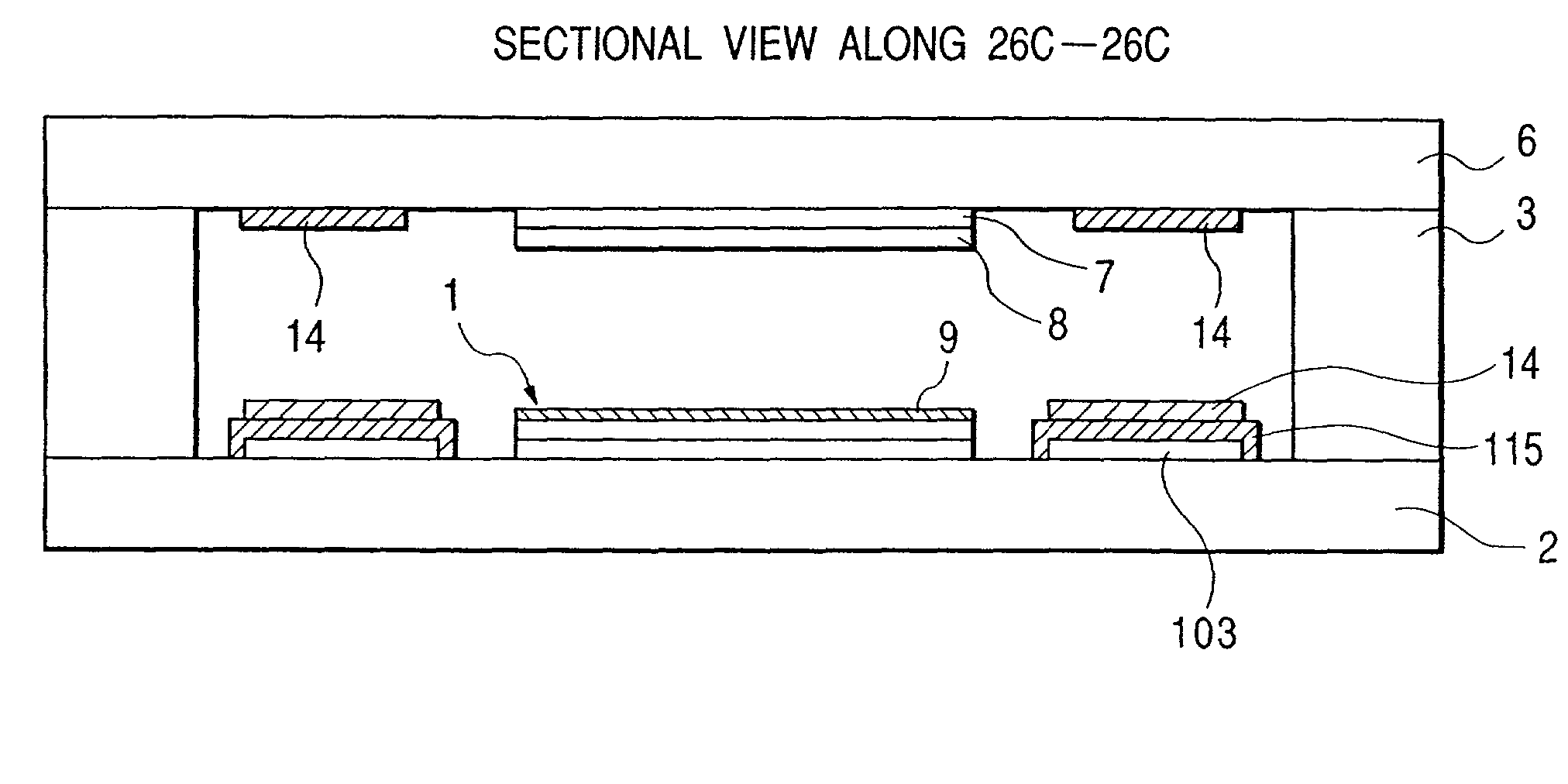
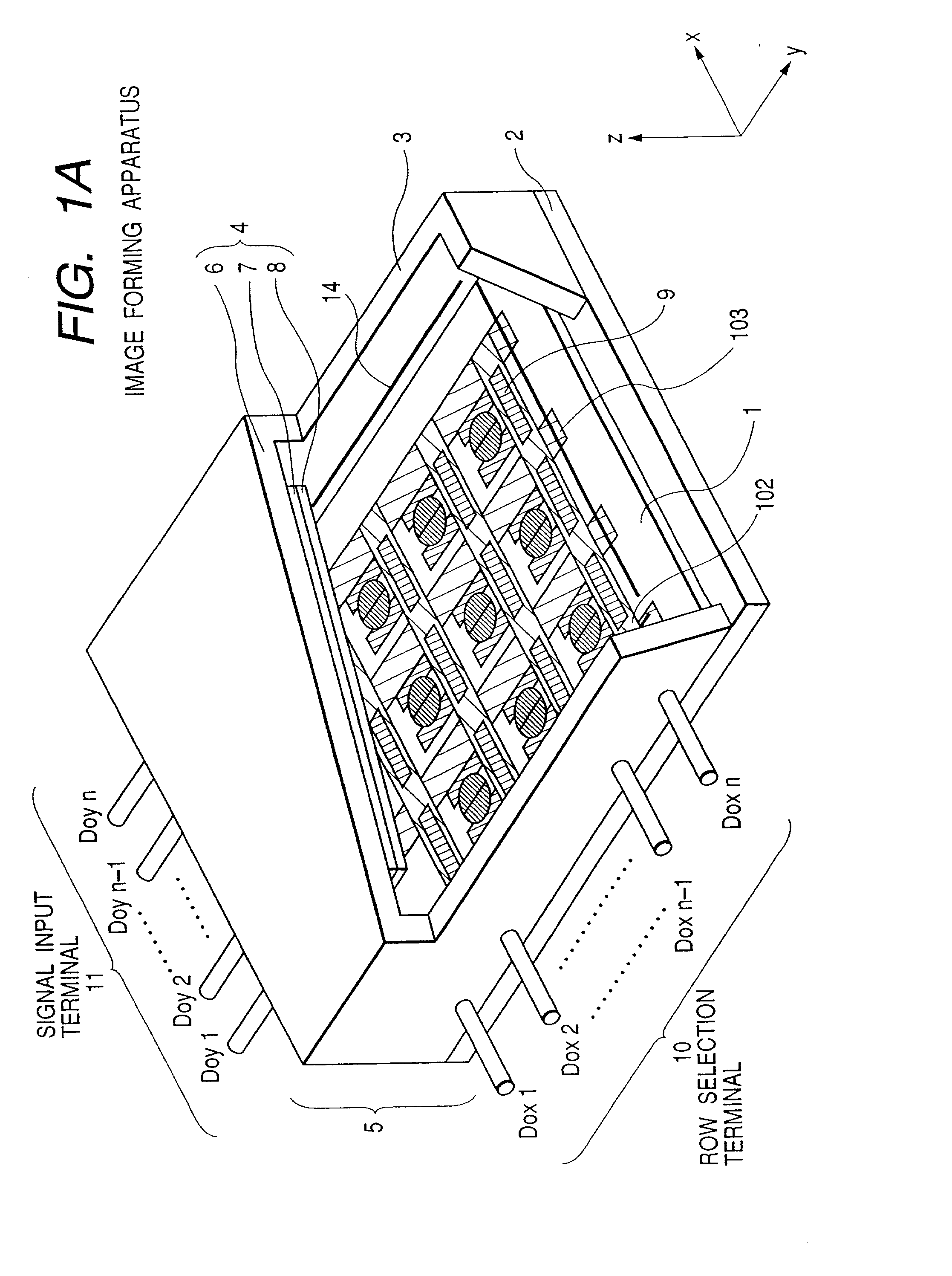
[0193] The image display apparatus of this embodiment is similar in configuration to that shown in FIGS. 5A to 5C, wherein the non-evaporating getters 9 are provided on the substantially entire surface of the row wirings (upper wirigns) 102 in the image display area and the non-evaporating getters 14 are provided on the insulation layer 115 covering the column wirings (lower wirings) 103 outside the image display area on the electron source substrate 1.
[0194] The image display apparatus of the present embodiment is provided, on the substrate 1, with an electron source consisting of plural surface conduction electron emitting elements wired in a simple matrix structure (100 rows.times.100 columns).
[0195] FIG. 21 is a partial plan view of the electron source substrate 1, while FIGS. 22A and 22B are cross-sectional views respectively along lines 22A-22A and 22B-22B in FIG. 21. A same component is represented by a same number in FIGS. 21, 22A and 22B. There are ...
seventh embodiment
[0233] [Seventh Embodiment]
[0234] FIGS. 23A to 23C show the image display apparatus of this embodiment.
[0235] In the present embodiment, the following step f-2 was executed between the steps f and g in the foregoing sixth embodiment.
[0236] Step f-2
[0237] The insulation film 115, consisting of a silicon oxide film of a thickness of 1.0 .mu.m, was deposited by RF sputtering also on the upper wirings 102 outside the image display area.
[0238] Also in the step x of the foregoing sixth embodiment, in forming the getters on the upper wirings 102 in the image display area and the lower wirings 103 outside the image display area, the getter layers 9, 14 consisting of a Ar--V--Fe alloy was formed by sputtering also on the insulation film 115 of the upper wirings 102 outside the image display area. The thickness of the getter layers 9, 14 was adjusted to 2 .mu.m. The sputtering target used had a composition of Zr 70%, V 25% and Fe 5% (ratio by weight).
[0239] Steps other than those mentioned ab...
PUM
 Abstract
Description
Claims
Application Information
 - R&D
- Intellectual Property
- Life Sciences
- Materials
- Tech Scout
- Unparalleled Data Quality
- Higher Quality Content
- 60% Fewer Hallucinations
Browse by: Latest US Patents, China's latest patents, Technical Efficacy Thesaurus, Application Domain, Technology Topic, Popular Technical Reports.
© 2025 PatSnap. All rights reserved.Legal|Privacy policy|Modern Slavery Act Transparency Statement|Sitemap|About US| Contact US: help@patsnap.com