Multi-layer chip directional coupler

Inactive Publication Date: 2002-08-15
SAMSUNG ELECTRO MECHANICS CO LTD
View PDF0 Cites 1 Cited by
  • Summary
  • Abstract
  • Description
  • Claims
  • Application Information

AI Technical Summary

Benefits of technology

[0013] Accordingly, the present invention has been made keeping in mind the above problems occurring in the prior art, and an object of the present invention is to provide a multi-layer chip directional coupler, in which a main signal line is asymmetrically formed to be shorter than a coupling signal line, thus simplifying the manufacturing process of the directional coupler, decreasing insertion loss.

Problems solved by technology

Therefore, because parts adapted to such mobile communication devices must satisfy the requirements for high frequency and narrow bandwidth, required design conditions are more and more complicated.
However, it is very difficult to accurately maintain the distance between the main signal line 3 and the coupling signal line 5 in the actual microstripline coupler.
Consequently, the conventional microstripline coupler is problematic in that it is very difficult to manufacture a coupler having highly coupled structure due to variation of the distance between the main signal line and the coupling signal line when the coupler is manufactured.
However, the conventional multi-layer chip directional coupler is problematic in that it has large insertion loss.

Method used


Image

  • Multi-layer chip directional coupler
  • Multi-layer chip directional coupler
  • Multi-layer chip directional coupler

Examples


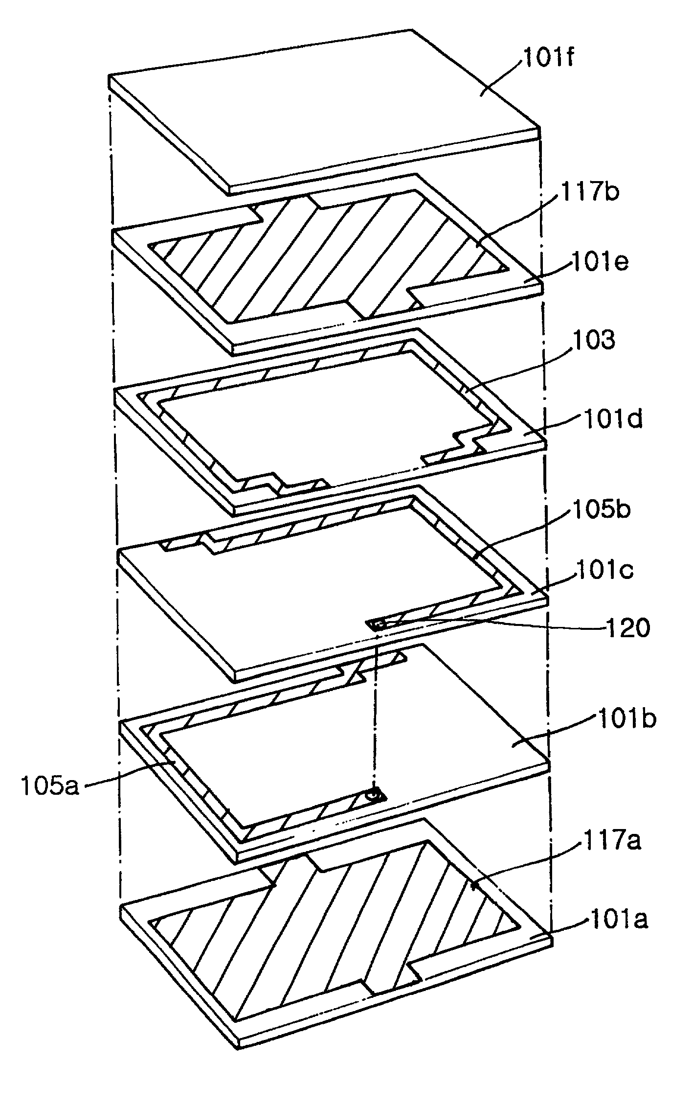
Embodiment Construction

1 4.30 6.16 183 237 0.244 14.2 1.083 Embodiment 2 3.55 6.16 116 225 0.231 14.3 1.134 Embodiment 3 2.52 6.16 94 253 0.183 15.6 1.153

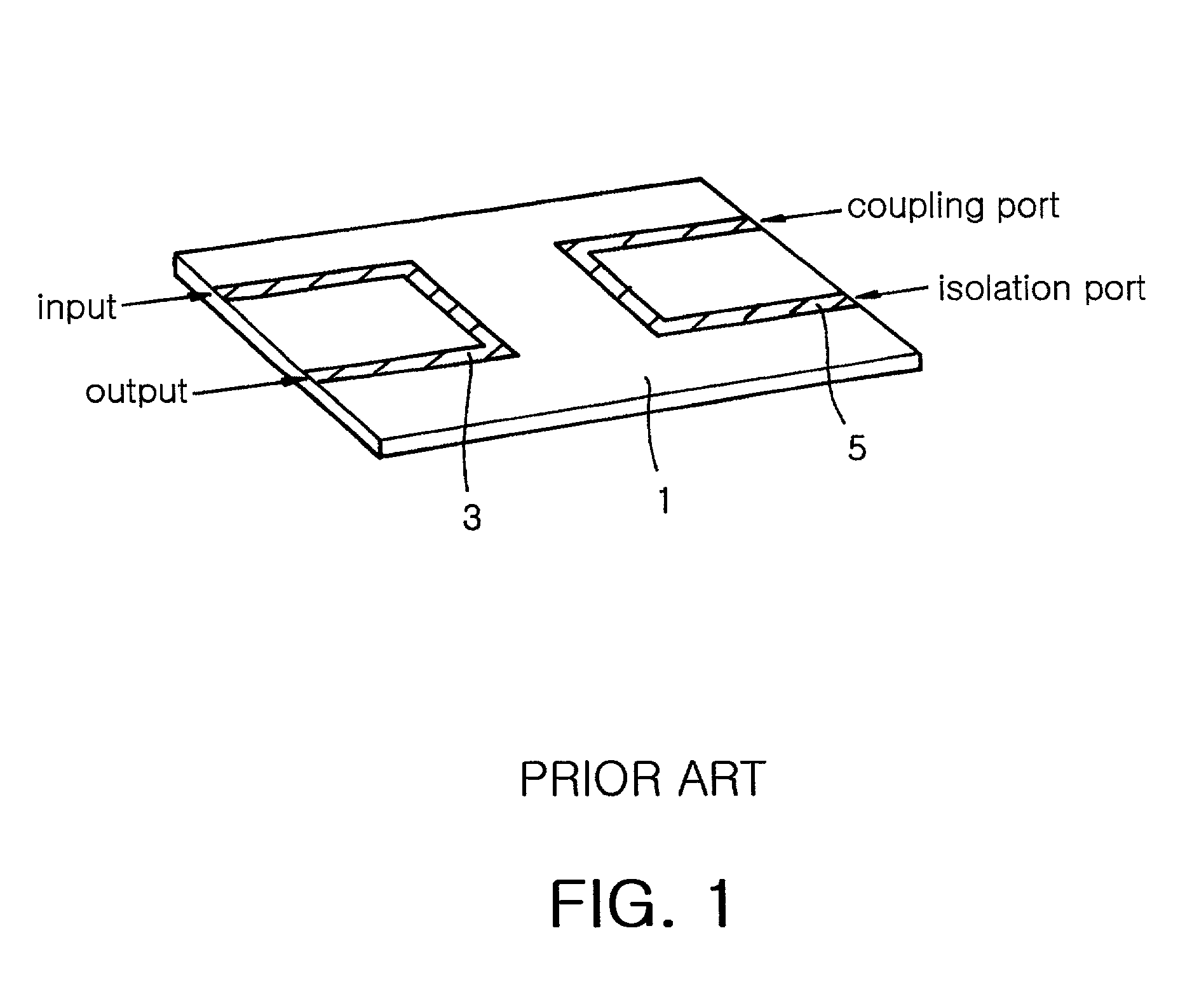
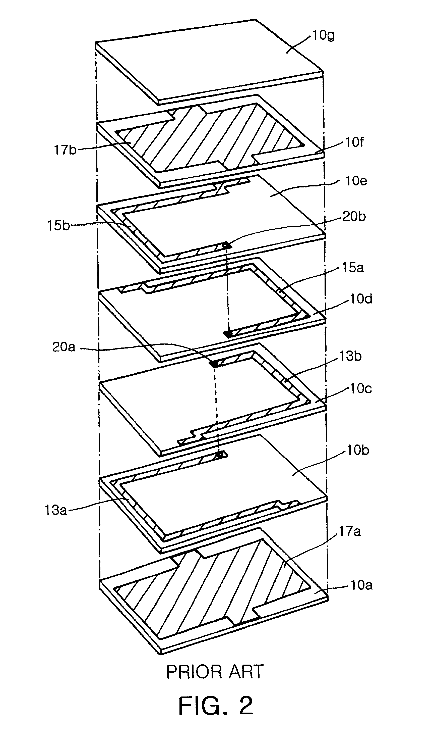
[0028] As shown in Table 1, four multi-layer chip directional couplers were manufactured such that their return losses were nearly the same. The four multi-layer chip directional couplers comprised dielectric substrates of the same size and same material. However, the four directional couplers were made to be different from each other in the length of each main signal line. In other words, in the directional coupler according to the comparative example, both the main signal line and the coupling signal line were constructed to have the same length, similarly to the conventional coupler having the symmetrical structure. On the other hand, in the directional couplers according to the first to third embodiments, the length of each main signal line was respectively set to 4.30 mm, 3.55 mm and 2.52 mm such that the main signal line was shorter than the coupli...


PUM


Abstract

Disclosed herein is a multi-layer chip directional coupler. The multi-layer chip directional coupler has a first ground pattern, a coupling signal line, a main signal line, a second ground pattern, and a plurality of ports. The first ground pattern is formed on the upper surface of a first dielectric layer. The coupling signal line is formed of a conduction pattern on the upper surface of a second dielectric layer. The main signal line is formed of a conduction pattern on the upper surface of a third dielectric layer formed over the second dielectric layer. The second ground pattern formed on the upper surface of a fourth dielectric layer formed over the third dielectric layer. A plurality of ports is formed on the side surfaces of the first to fourth dielectric layers.

Description

[0001] 1. Field of the Invention[0002] The present invention relates generally to directional couplers, and more particularly to a multi-layer chip directional coupler, in which a main signal line layer is formed on one dielectric layer, such that the main signal line layer is shorter than a coupling signal line layer formed on two dielectric layers, thus decreasing resistance of a conduction pattern and reducing insertion loss.[0003] 2. Description of the Prior Art[0004] Recently, as mobile communication fields are rapidly developed, a usable frequency becomes higher and its bandwidth becomes narrower. Therefore, because parts adapted to such mobile communication devices must satisfy the requirements for high frequency and narrow bandwidth, required design conditions are more and more complicated.[0005] A directional coupler used in the mobile communication devices serves to divide transmission signals at a constant rate. Especially, in the directional coupler, a certain amount of ...

Claims


Application Information

Patent Timeline
IPC IPC(8): H01P5/18
CPCH01P5/185H01P5/18
Inventor SHIN, JI-HWANJEONG, SEUNG-GYO
Owner SAMSUNG ELECTRO MECHANICS CO LTD
Why Eureka
Try Eureka