PLL device

a technology of pll and pll plate, which is applied in the direction of electrical equipment, pulse automatic control, etc., can solve the problems of high manufacturing cost, easy failure of lock, and inability to smooth the establishment of lock

Inactive Publication Date: 2002-08-29
SANYO ELECTRIC CO LTD +1
View PDF0 Cites 4 Cited by
  • Summary
  • Abstract
  • Description
  • Claims
  • Application Information

AI Technical Summary

Problems solved by technology

The inventor tried to track down the cause, and found it to be that the phase comparators interfered with each other as a locked state approached, which prevented smooth establishment of lock.
It is also found that since the conventional PLL device switches the phase comparators to be in use from multiple stages to a single stage when the locked state approaches, that is, since the gate of one phase comparator is kept open and the gates of the other phase comparators are closed, closing and opening timings of the gates have to be extremely precise, and therefore, it has a disadvan...

Method used


Image

  • PLL device
  • PLL device
  • PLL device

Examples


first embodiment

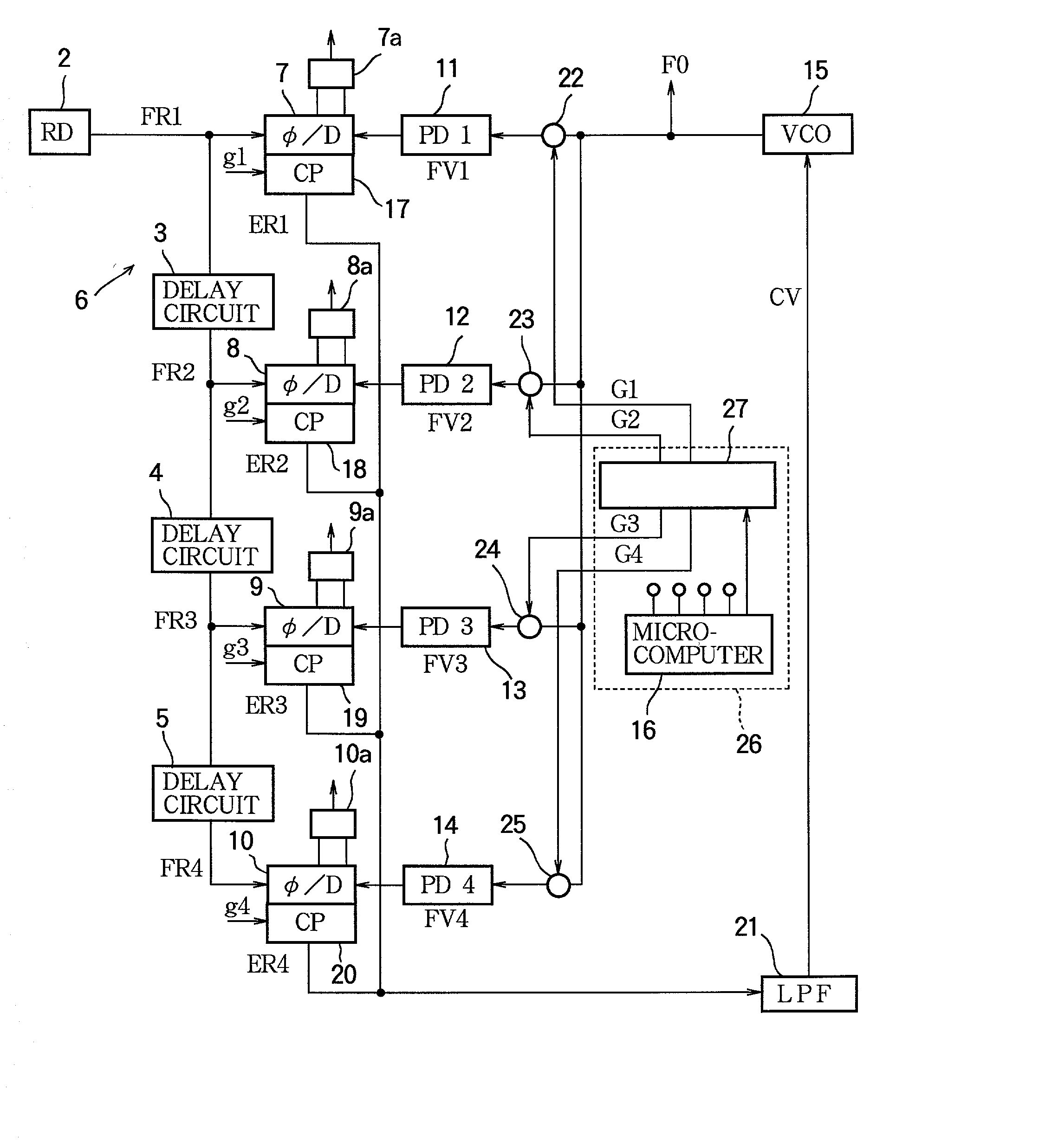
[0080] A PLL device according to the invention will be explained below with reference to a block diagram of FIG. 1. In FIG. 1, a reference oscillator 2 outputs a reference signal FR1. Delay circuits 3, 4, 5 produce a plurality of reference signals FR2, FR3, FR4 having mutually differing phases in response to the reference signal FR1. This reference oscillator 2 and the delay circuits 3, 4, 5 constitute a (reference signal) generating means 6.

[0081] To be more specific, the reference signal FR1 is input into a phase comparator 7. The delay circuit 3 delays the reference signal FR1 by 1 / 4 period, and outputs it as the reference signal FR2 to a phase comparator 8. The delay circuit 4 delays the reference signal FR1 by 1 / 2 period, and outputs it as the reference signal FR3 to a phase comparator 9. The delay circuit 5 delays the reference signal FR1 by 3 / 4 period, and outputs it as the reference signal FR4 to a phase comparator 10.

[0082] Variable frequency dividers 11, 12, 13, 14 whose i...

second embodiment

[0123] A PLL device according to the invention will be explained with reference to a block diagram of FIG. 4. In FIG. 4, the elements that are the same as those in FIG. 1 are given the same reference characters, and explanation thereof will be omitted.

[0124] Phase comparators 57 to 60 will be explained in detail with reference to FIG. 4 to FIG. 6. The phase comparators 57 to 60 are divided into at least two groups. For example, the phase comparator 57 is a first phase comparator, and the phase comparators 58, 59, 60 are second phase comparators. FIG. 5 is a circuit diagram of the second phase comparator, and FIG. 6 is a view showing characteristics of the phase comparators 57 to 60.

[0125] The second phase comparators 58, 59, 60 will be explained with reference to the diagram of FIG. 5. In FIG. 5, a first delay circuit 40 is constituted by, for example, a series circuit of a plurality of inverters. The first delay circuit 40 has an input connected to a first input terminal 41, and an...

third embodiment

[0159] A PLL device 1 according to the invention will be explained with reference to FIG. 7. In FIG. 7, the elements that are the same as those in FIG. 1 are given the same reference characters, and explanation thereof will be omitted.

[0160] Phase comparators 67 to 70 will be explained in- detail with reference to FIG. 7 and FIG. 8. FIG. 7 is a block diagram of the phase comparators 68, 69, 70. In these FIGS., for example, a delay circuit 60 is constituted by four inverters connected in series, a delay circuit 61 is constituted by six inverters connected in series, and a delay circuit 62 is constituted by eight inverters connected in series.

[0161] The delay circuits 60, 61, 62 constituted by different numbers of inverters have different delay times.

[0162] One end of each of the delay circuits 60, 61, 62 is coupled to a common input. To be more specific,the one end is connected to a first input terminal 63 which receives a reference signal FR.

[0163] The other end of each of the delay...


PUM


Abstract

The PLL device includes means (6) for generating a, plurality of reference signals (FR1, FR2, FR3, FR4) having mutually differing phases, a variable frequency divider (11, 12, 13, 14) for dividing, in synchronization with the phases of a plurality of the reference signals, a frequency of an output signal (FO) of a voltage-controlled oscillator (15) that produces a signal having a frequency responsive to a control voltage (CV) supplied to generate a plurality of feedback signals (FV1, FV2, FV3, FV4) having mutually differing phases, phase comparators (7, 17, 8, 18, 9, 19, 10, 20) for comparing phases between the reference signals and the feedback signals corresponding to the reference signals respectively to produce a plurality of error signals (ER1, ER2, ER3, ER4), a low-pass filter (21) for filtering the error signals output from the phase comparators to produce the control voltage, and a control means (16, 26, 27) for controlling the number of the phase comparators that output the error signals to the low-pass filter in accordance with a phase difference between at least one of a plurality of the feedback signals and the reference signal corresponding to the one of a plurality of the feedback signals.

Description

[0001] 1. Field of the Invention[0002] The present invention relates to a PLL device.[0003] 2. Background Art[0004] As shown, for example, in the drawing at page 32 of "SANYO TECHNICAL REVIEW" Vol.10, No.1, February 1978, a PLL device that generates signals of various frequencies from a reference signal having a certain frequency is known. Such a PLL device includes a reference oscillator generating a reference signal RF, a voltage-controlled oscillator generating an output signal FO responsive to a control voltage CV, a variable frequency divider dividing the frequency of the output signal FO to generate a feedback signal FV, a phase comparator comparing the phase of the feedback signal FV with the phase of the reference signal to generate an error signal ER, and a low-pass filter generating the control voltage CV in response to the error signal ER.[0005] The locking time in this PLL device, or the time needed to synchronize the output signal with the reference signal in phase is d...

Claims


Application Information

Patent Timeline
IPC IPC(8): H03L7/08H03L7/087H03L7/089H03L7/095H03L7/107H03L7/183H03L7/191H03L7/199
CPCH03L7/0802H03L7/087H03L7/0891H03L7/0898H03L7/095H03L7/107H03L7/1077H03L7/183H03L7/191H03L7/199H03L2207/04H03L2207/18H03L7/1072
Inventor SUMI, YASUAKIHORIKOSHI, KATSUUCHIYAMA, HISAYOSHI
Owner SANYO ELECTRIC CO LTD
Why Eureka
Try Eureka