Liquid crystal display device and its manufacturing method

a technology of liquid crystal display and manufacturing method, which is applied in the direction of identification means, instruments, optics, etc., can solve the problems of deterioration of display quality, difficulty in realizing high aperture ratio, and decreasing brightness

Inactive Publication Date: 2002-08-29
BEIHAI HKC OPTOELECTRONICS TECH CO LTD
View PDF6 Cites 19 Cited by
  • Summary
  • Abstract
  • Description
  • Claims
  • Application Information

AI Technical Summary

Problems solved by technology

Such liquid crystal alignment defect appears as a line or dot detect, resulting in deterioration of display quality.
However, if the width of the black matrix is too wide, there occurs difficulty in setting an aperture ratio of liquid crystal display element largely, thereby decreasing brightness Here, the aperture ratio means the percentage of a pixel area contributing to optical modulation to the entire surface area of the display area of a liquid crystal display panel.
At the occasion of pushing forward high definition, the use of CF-On TFT structure makes it difficult to realize the high aperture ratio for the following reason.

Method used


Image

  • Liquid crystal display device and its manufacturing method
  • Liquid crystal display device and its manufacturing method
  • Liquid crystal display device and its manufacturing method

Examples


Embodiment Construction

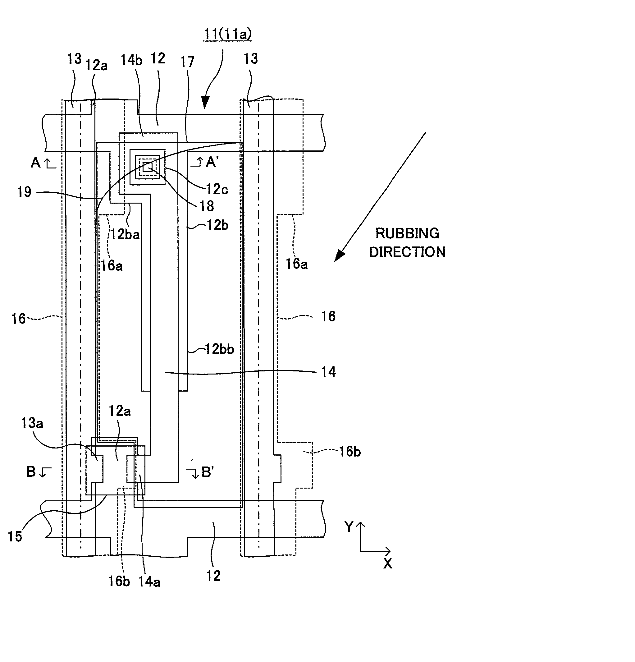
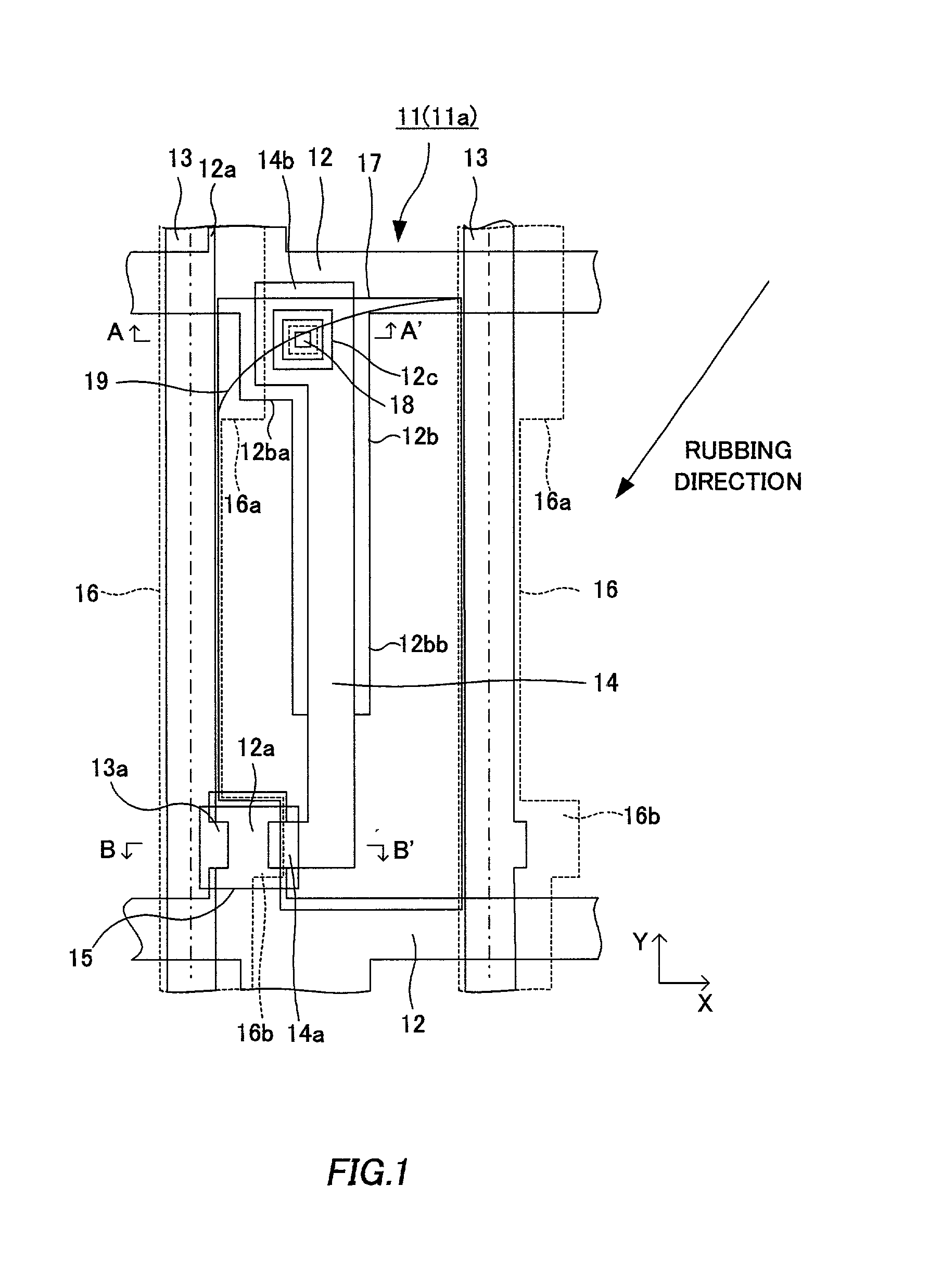
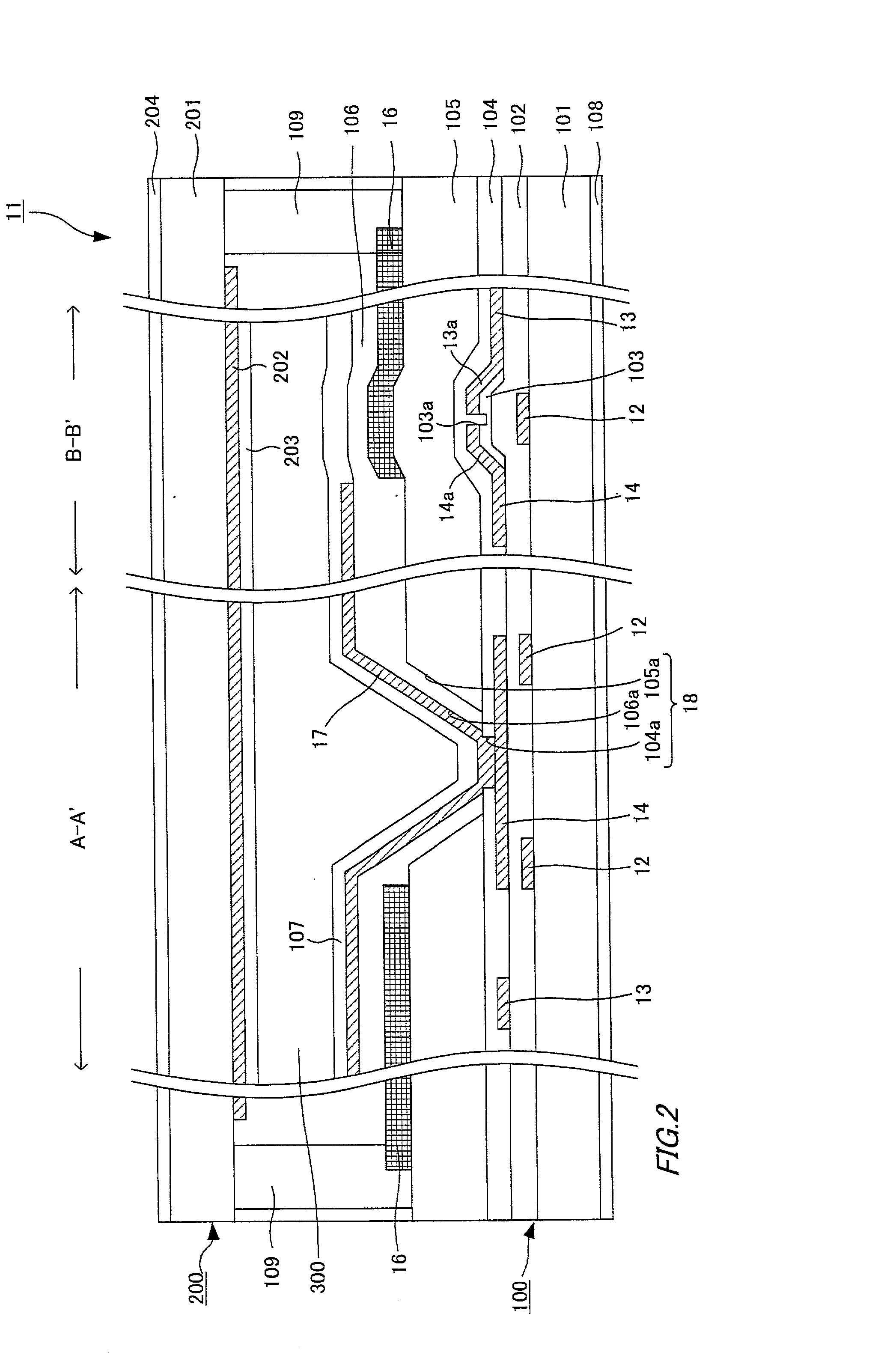
[0101] We studied the reduction in aperture ratio with high definition by examining the relationship between the pixel pitch and area ratio of contact hole 18. The result is shown in FIG. 4.

[0102] FIG. 4 shows the result of studying the liquid crystal display device in which the contact hole 18 does not overlap the disclination line 19 as illustrated in FIG. 5. The structure illustrated in FIG. 5 has substantially the same structure as illustrated in FIG. 1 excepting the position of contact hole 18.

[0103] Moreover, in FIG. 5, it is assumed that the contact hole 18 has a square cross section and an outer diameter of 14 .mu.m.times.14 .mu.m regardless of the size of pixel. This outer diameter value is a value obtained when the outer diameter of opening of passivation layer 104 is 8 .mu.m.times.8 .mu.and each side of the overlapping margin of overcoat layer 106 and color layer 105 is 1.5 .mu.m. At this time, it is assumed that one contact hole 18 with a cross-sectional area of 196 .mu....


PUM

PropertyMeasurementUnit
outer diameteraaaaaaaaaa
areaaaaaaaaaaa
area ratioaaaaaaaaaa

Abstract

In an active matrix type liquid crystal display device comprising a TFT having gate lines and data lines formed in a matrix manner and being connected to a source line, a contact hole for connecting the source line with a pixel electrode is formed in a position overlapping a disclination line. The contact hole is formed in a position overlapping a capacitance portion of the gate line. The gate line and the source line are provided to oppose to each other, and electrostatic capacitance is stored therebetween.

Description

[0001] 1. Field of the Invention[0002] The present invention relates to a liquid crystal display device and its manufacturing method, and particularly relates to an active matrix type liquid crystal display device having a color filter on its element substrate and its manufacturing method.[0003] 2. Description of the Related Art[0004] The active matrix liquid crystal display device comprises an element substrate with a switching element such as a transistor, etc., an opposite substrate arranged to be opposite to the element substrate, and a liquid crystal filled between the element substrate and opposite substrate.[0005] The opposite substrate has a color filter (CF) and a black matrix. The color filer consists of color layers of red, green or blue arranged regularly. The black matrix is formed of a film with a light shielding property (opaque). The black matrix shields disclination of the liquid crystal to prevent a reduction in contrast.[0006] The liquid crystal is filled in a spa...

Claims


Application Information

Patent Timeline
Patent Type & Authority Applications(United States)
IPC IPC(8): G02B5/00G02B5/20G02F1/1335G02F1/1337G02F1/136G02F1/1362G02F1/1368G09F9/30
CPCG02F1/136209G02F1/136227G02F2001/13373G02F2001/136222G02F1/13373G02F1/136222G02F1/136
Inventor HIDEHIRA, MASANOBUSAKAMOTO, MICHIAKIKUROHA, SHOUICHIOKAMOTO, MAMORU
Owner BEIHAI HKC OPTOELECTRONICS TECH CO LTD
Why Eureka
Try Eureka