Assembling arrays of small particles using an atomic force microscope to define ferroelectric domains

a technology of atomic force microscope and ferroelectric domain, which is applied in the field of structure with functional length scale, can solve the problems of difficult manipulation of nanoscale elements, difficult to modulate nanoparticle/substrat interaction, and formidable challenge of magnetic storage system

Inactive Publication Date: 2002-08-29
IBM CORP
View PDF0 Cites 22 Cited by
  • Summary
  • Abstract
  • Description
  • Claims
  • Application Information

AI Technical Summary

Problems solved by technology

Although significant switching characteristics have been demonstrated in these systems, the assembly, interconnection and addressing of such nanostructures for logic or memory chips, magnetic storage systems remains a formidable challenge.
This is a consequence of the difficulties of manipulation of nanoscale elements even in a laboratory environment.
Unfortunately, the art lacks technique

Method used


Image

  • Assembling arrays of small particles using an atomic force microscope to define ferroelectric domains
  • Assembling arrays of small particles using an atomic force microscope to define ferroelectric domains
  • Assembling arrays of small particles using an atomic force microscope to define ferroelectric domains

Examples


Embodiment Construction

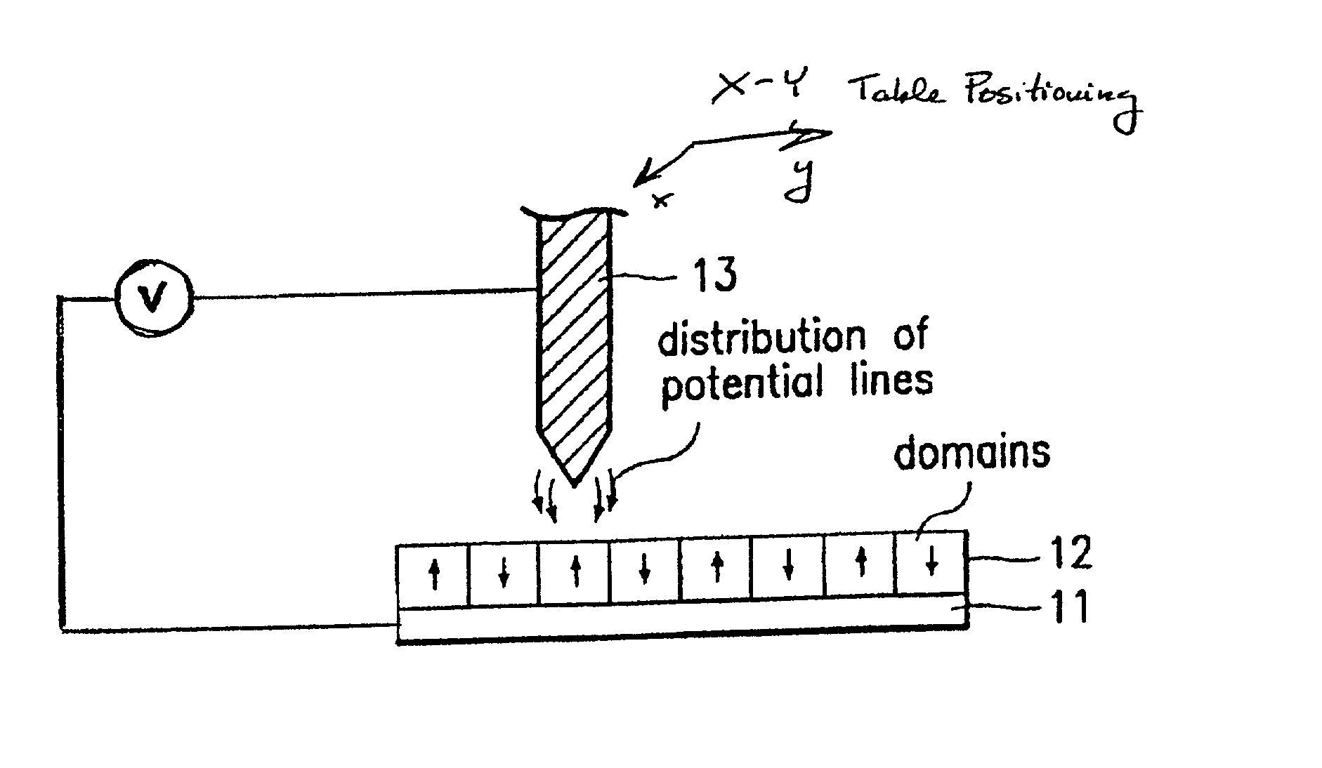
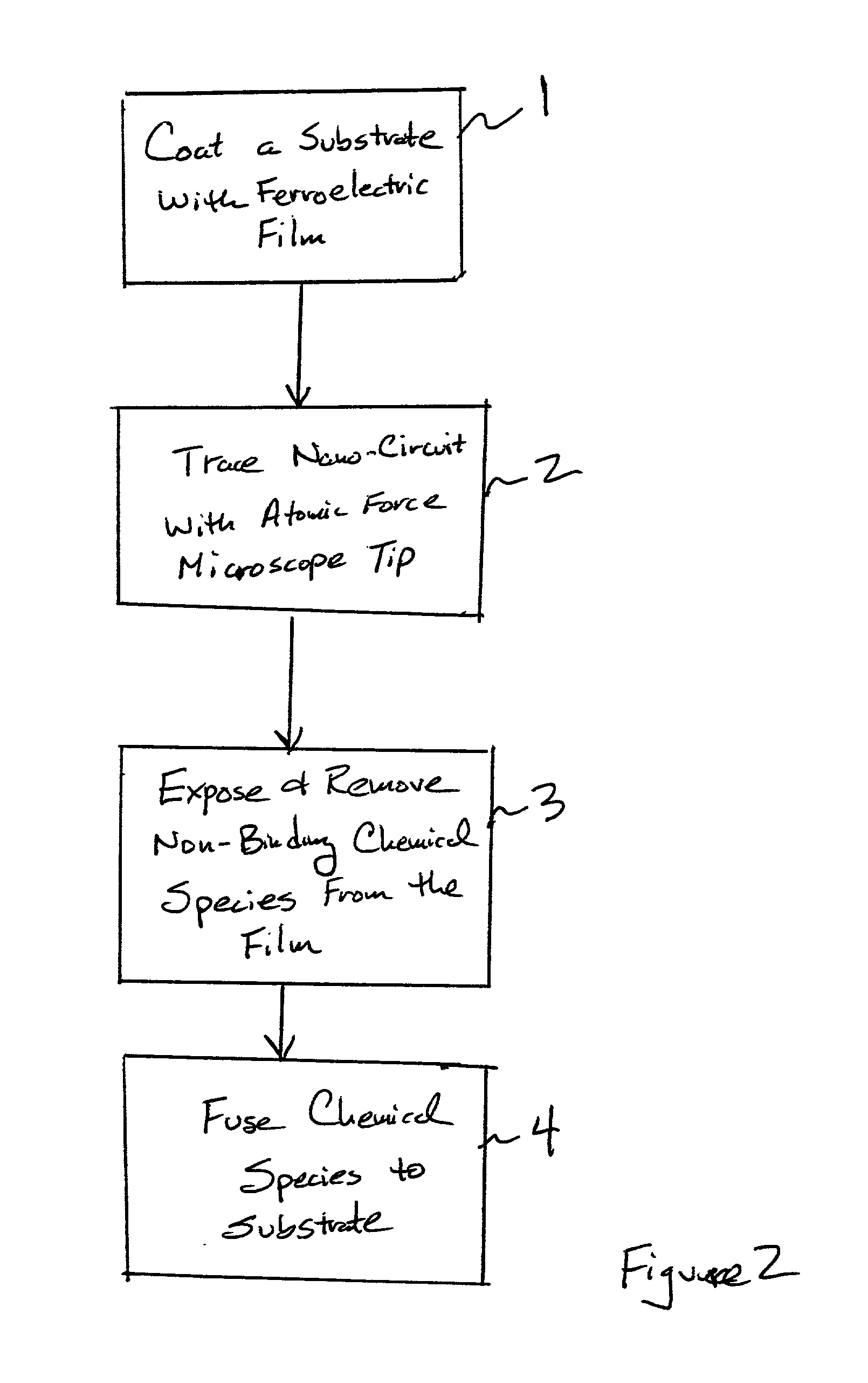
[0016] In referring now to FIGS. 1 and 2, the invention provides a method of producing a structure by pre-patterning a surface with nanoscale resolution to assemble structures of nanoparticles, molecules, or localized products of molecular decomposition. Stable ferroelectric domains on the nanometer scale can be prepared in various states of remnant polarization by use of an atomic force microscope (AFM) using a properly biased metal tip. This allows persistent patterning of the surface potential with nanoscale resolution which is then used to draw a locus where nanoparticles or molecules are induced to assemble by the strong localized electrostatic interaction when deposited from a solution with non-polar solvent, or where selective molecular decomposition in a CVD process occurs. The proximity of two oppositely polarized surface regions and the magnitude of the polarization can be adjusted to control the relative field strengths at the surface and thereby control the deposition of...


PUM


Abstract

A method of assembling arrays of small particles or molecules using an atomic force microscope to define ferroelectric domains includes depositing a ferroelectric thin film upon a substrate forming workpiece, then using an atomic force microscope having a conductive, tip for generating a pattern on this thin film to define desired nano-circuit patterns. Next, exposure of this thin film to a solution containing chemical species which selectively adsorb or accumulate under the influence of electrophoretic forces in selected regions of this thin film.

Description

[0001] 1. Field of the Invention[0002] The present invention generally relates to structures with functional length scales measured in nanometers, and more particularly, to methods of making the same. The nanostructured assemblies may have application in electronic, optical, and magnetic storage devices.[0003] 2. Description of the Related Art[0004] As the limits in miniaturization of silicon based electronic devices and magnetic storage systems appear on the horizon, new generations of nano-devices are attracting attention. Contenders in the nanoscale world of electronics and storage technology include single electron transistors, nanotubes, molecular wire crossbar memory, nanoscale patterned magnetic arrays and so on. Although significant switching characteristics have been demonstrated in these systems, the assembly, interconnection and addressing of such nanostructures for logic or memory chips, magnetic storage systems remains a formidable challenge. This is a consequence of th...

Claims


Application Information

Patent Timeline
IPC IPC(8): G01B11/16G01Q60/00G01Q80/00B82B3/00G11B5/85G11B5/851H01L21/027H01L21/8246H01L27/105
CPCG01B11/165Y10S977/962Y10S977/869Y10S977/881Y10S977/863Y10S977/859
Inventor MISEWICH, JAMESMURRAY, CHRISTOPHER B.SCHROTT, ALEJANDRO G.
Owner IBM CORP
Why Eureka
Try Eureka