Vacuum atomic force microscope and using method thereof

An atomic force microscope and vacuum technology, applied in the direction of measuring devices, instruments, scientific instruments, etc., can solve the problems of small scanning range of the microscope and scanning of difficult-to-select areas, and achieve the effect of overcoming design difficulties, large scanning range and high resolution

Inactive Publication Date: 2010-01-13
SUZHOU INST OF NANO TECH & NANO BIONICS CHINESE ACEDEMY OF SCI
View PDF0 Cites 18 Cited by
  • Summary
  • Abstract
  • Description
  • Claims
  • Application Information

AI Technical Summary

Problems solved by technology

[0005] In view of the inconvenience in the design and use of the above-mentioned existing atomic force microscope using laser positioning in a vacuum environment, the purpose of the present invention is to design a vacuum atomic force micros

Method used


Image

  • Vacuum atomic force microscope and using method thereof
  • Vacuum atomic force microscope and using method thereof
  • Vacuum atomic force microscope and using method thereof

Examples


Embodiment Construction

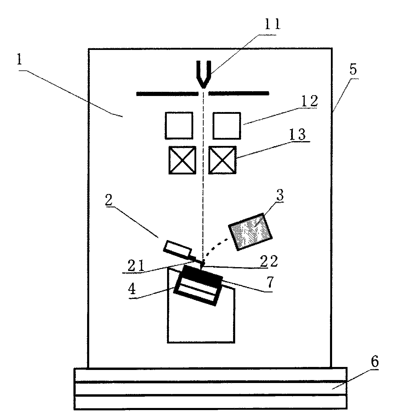
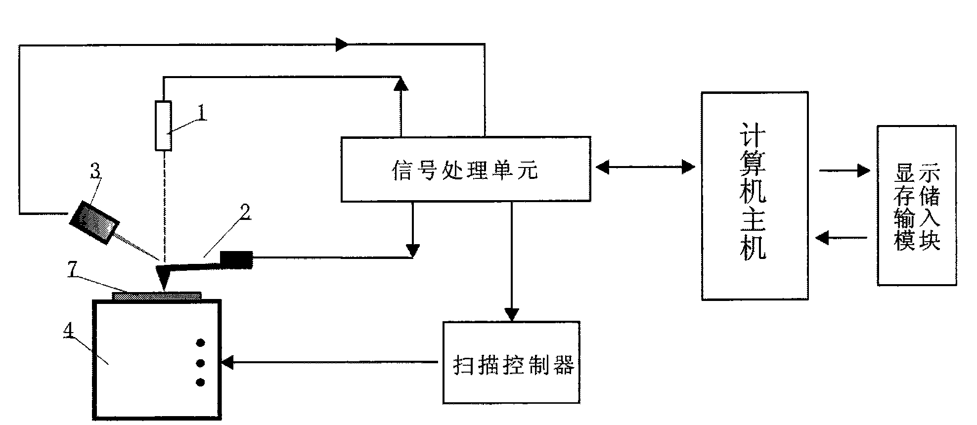
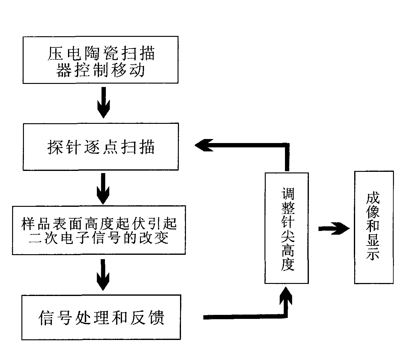
[0019] like figure 1 As shown in the schematic structural diagram of a specific embodiment of the vacuum atomic force microscope system of the present invention, the atomic force microscope mainly includes a feedback controller, a shock absorber 6 at the bottom, a vacuum chamber 5 connected to the shock absorber 6, and a vacuum chamber 5 disposed in the vacuum chamber 5 The electron beam emitting device 1, the probe 2, the secondary electron receiver 3 and the piezoelectric ceramic scanner 4, wherein:

[0020] The electron beam emitting device is composed of an electron gun 11 , an electromagnetic lens 12 and a scanning coil 13 . The electron gun 11 is used to generate electron beams; the electromagnetic lens 12 mainly plays the role of converging, which can focus and reduce the electron beam spot step by step; the scanning coil 13 can be used to control the position of the electron beam irradiation.

[0021] The secondary electron detector 3 is used to detect the secondary e...


PUM


Abstract

The invention discloses a vacuum atomic force microscope and a using method thereof, belonging to the field of micro-topography detecting equipment; the microscope comprises an electron beam launching device, a secondary electron detector, a probe with a cantilever, a piezoelectric ceramics scanner and a feedback controller. When in work, electron beams are irradiated to the cantilever of the probe; as the acting force between the probe and sample atoms causes the cantilever to become deformed; a secondary electron signal changes; the acting force between a pinpoint and the sample is controlled to be constant by the signal feedback; the pinpoint scans the surface of the sample point by point and can image surface topography of the sample. The currently common optical lever does not need to be drawn into the invention; the invention overcomes design difficulty brought about by the conventional atomic force microscope applied in vacuum environment, synthesizes two nanophase material characterization methods which are the advantages of the atomic force microscope and an electronic microscope, and can realize the continuous measuring on the material from millimeter size to the sub-nanometer size.

Description

technical field [0001] The invention relates to a microscope device, in particular to an atomic force microscope system applied in a vacuum environment, and belongs to the field of microscopic topography detection equipment. Background technique [0002] Atomic force microscopy can image the surfaces of conductors, semiconductors, and insulators with micro-nano precision, and is a powerful characterization method in physics, chemistry, biology, and materials science. Atomic force microscopes work on the basis of atom-to-atom interaction forces. When a very sharp micro-probe at the front end of the cantilever is sufficiently close to the sample surface in the longitudinal direction to a distance of several nanometers or even smaller, an atomic force will be generated between the atoms at the tip of the micro-probe and the atoms on the sample surface. There is a certain curve relationship between the size of the atomic force and the distance, and the microscopic topography of...

Claims


Application Information

Patent Timeline
IPC IPC(8): G01N13/16G12B21/08
CPCG01Q30/16
Inventor 秦华刘争晖钟海舰樊英民徐科
Owner SUZHOU INST OF NANO TECH & NANO BIONICS CHINESE ACEDEMY OF SCI
Why Eureka
Try Eureka