Piezoelectric/electrostrictive device and method of fabricating the same

a technology of electroelectric and electrodestriction, which is applied in the direction of device details, instruments, and piezoelectric/electrostrictive devices, etc., can solve the problems of deformation of the deformable portion, the inability to perform stably deflecting the reflective surface over a long period of time, and the difficulty of maintaining flatness of the reflective surface implemented by the light-reflecting member 318

Inactive Publication Date: 2002-09-05
NGK INSULATORS LTD
View PDF0 Cites 19 Cited by
  • Summary
  • Abstract
  • Description
  • Claims
  • Application Information

AI Technical Summary

Problems solved by technology

Also, since the light-reflecting member 318 is formed of a thin metal film, whose rigidity is low, the reflective surface implemented by the light-reflecting member 318 encounters difficulty in maintaining flatness.
Since the flatness of the reflective surface changes with time as a result of operation of the AMA, the operation of deflecting the reflective surface cannot be performed stably over a long period of time.
Therefore, the deformable portion is unlikely to deteriorate with time.
Thus, the AMA encounters difficulty in maintaining good flatness of the reflective surface over a long period of time.
However, such a dimensional relationship is not the only means for preventing deformation of the reflective portion 13.
Such materials are likely to react with a piezoelectric / electrostrictive material during heat treatment of a piezoelectric / electrostrictive layer, causing the material composition to vary with a resultant deterioration in piezoelectric characteristics.

Method used


Image

  • Piezoelectric/electrostrictive device and method of fabricating the same
  • Piezoelectric/electrostrictive device and method of fabricating the same
  • Piezoelectric/electrostrictive device and method of fabricating the same

Examples


Embodiment Construction

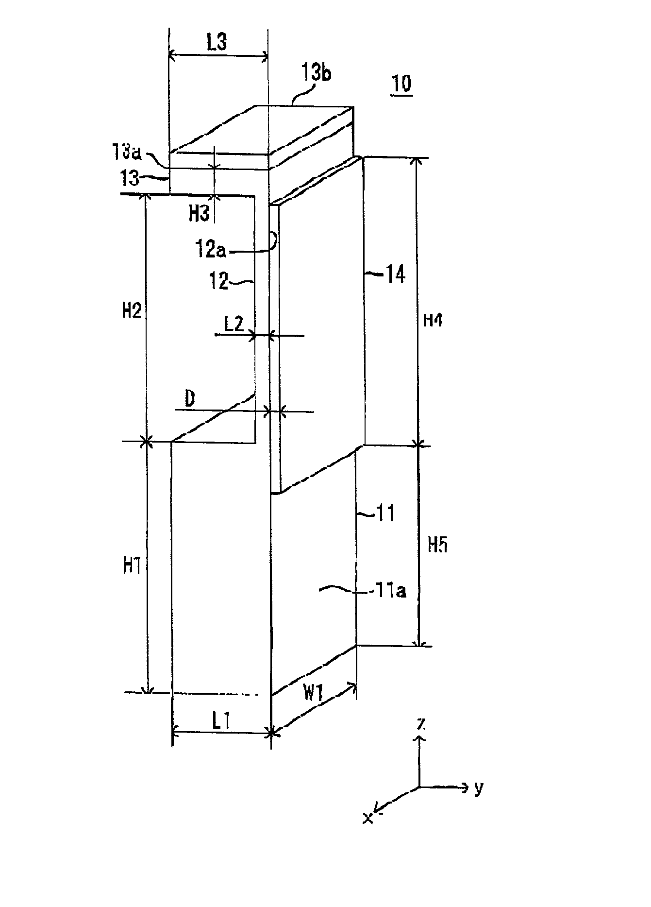
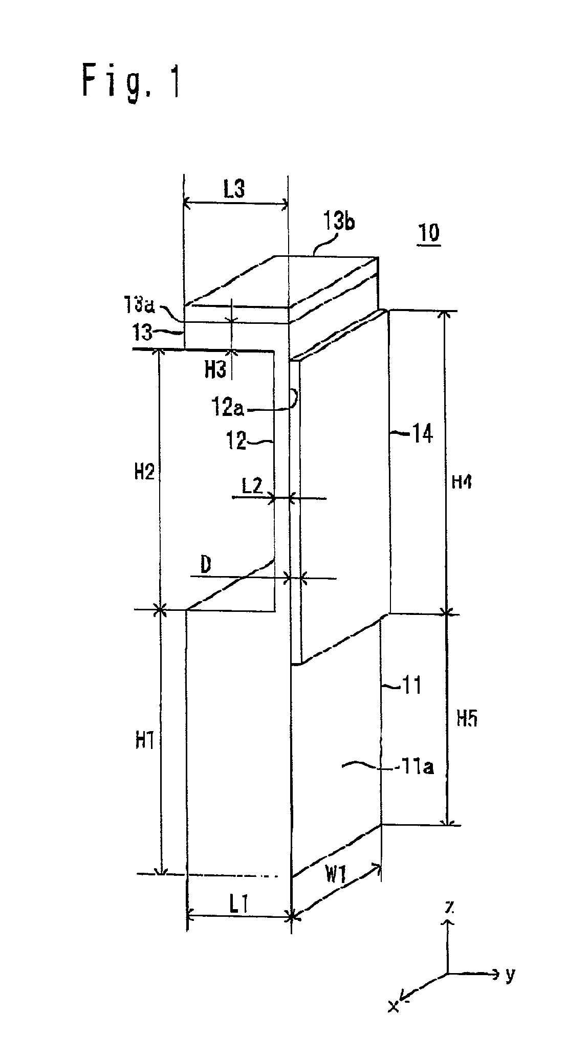
[0209] A specific example of application of the piezoelectric / electrostric-tive device 30 of the third embodiment to an optical switch will next be described. The application to an optical switch described below is also applicable to other embodiments mentioned above.

[0210] A piezoelectric / electrostrictive device 130 shown in FIG. 31 includes the piezoelectric / electrostrictive device 30 and a stopper member 22. The stopper member 22 is disposed above the light-reflecting members 13b of the piezoelectric / electrostrictive device 30 in such a manner as to be in parallel with the reflective surfaces of the light-reflecting members 13b when the deformable portions 12 are not displaced. The stopper member 22 is a transparent (light-transmitting) thin plate of, for example, glass, quartz, or transparent plastic (e.g., acrylic). The stopper member 22 is positioned such that, when the active plane 13a of a certain reflective portion 13 (accordingly, the reflective surface of the correspondin...


PUM

PropertyMeasurementUnit
temperatureaaaaaaaaaa

Abstract

A piezoelectric/electrostrictive device includes a functional element. The functional element includes a base portion; a deformable portion assuming the form of a thin plate and extending from the base portion to thereby form a plane; a piezoelectric/electrostrictive element formed on the deformable portion; and a reflective portion extending from the deformable portion so as to form an active plane intersecting with the plane of the deformable portion, and having a light-reflecting member disposed on the active plane. Operation of the piezoelectric/electrostrictive element causes the deformable portion to be deformed in a direction substantially perpendicular to the plane of the deformable portion to thereby change a reflection angle of light reflected from the reflective portion.

Description

[0001] 1. Field of the Invention[0002] The present invention relates to a piezoelectric / electrostrictive device having a light modulation mechanism for use in an image display unit, an image printing unit, an exposure unit, an optical switch, or a like apparatus.[0003] 2. Description of the Related Art[0004] Recently, various devices having light modulation mechanisms have been developed. For example, Japanese Patent Application Laid-Open (kokai) No. 5-196880 discloses a deformable mirror device (hereinafter called a DMD). As shown in the schematic perspective view of FIG. 33, the DMD includes a CMOS substrate 200; two support elements 202 disposed on the substrate 200; a pair of torsion hinges 204 supported by the support elements 202; a yoke 206 supported by the support elements 202 via the torsion hinges 204; and a mirror 208 supported by the yoke 206. The torsion hinges 204 are twisted through utilization of electrostatic attraction, to thereby change the angle of the mirror 208...

Claims


Application Information

Patent Timeline
Patent Type & Authority Applications(United States)
IPC IPC(8): G02B26/08H01L41/04H01L41/08H01L41/09H01L41/314H01L41/338H02N2/02H04R17/00
CPCG02B26/0858H01L41/094H01L41/0946H01L41/314H01L41/338Y10T29/49002Y10T29/4908Y10T29/42Y10T29/4902Y10T29/49005H10N30/2043H10N30/2042H10N30/074H10N30/088
Inventor TAKEUCHI, YUKIHISANANATAKI, TSUTOMUKIMURA, KOJI
Owner NGK INSULATORS LTD
Why Eureka
Try Eureka