

Multi-bit test circuit
a multi-bit test and test circuit technology, applied in the field of multi-bit test circuits, can solve the problems of wasting time, wasting time, and wasting time in executing the test, so as to reduce the interconnection line length of teacher data, reduce the driven load of teacher data, and accelerate timing
- Summary
- Abstract
- Description
- Claims
- Application Information
AI Technical Summary
Benefits of technology
Problems solved by technology
Method used
Image

Examples
first embodiment
[0030] [First Embodiment]
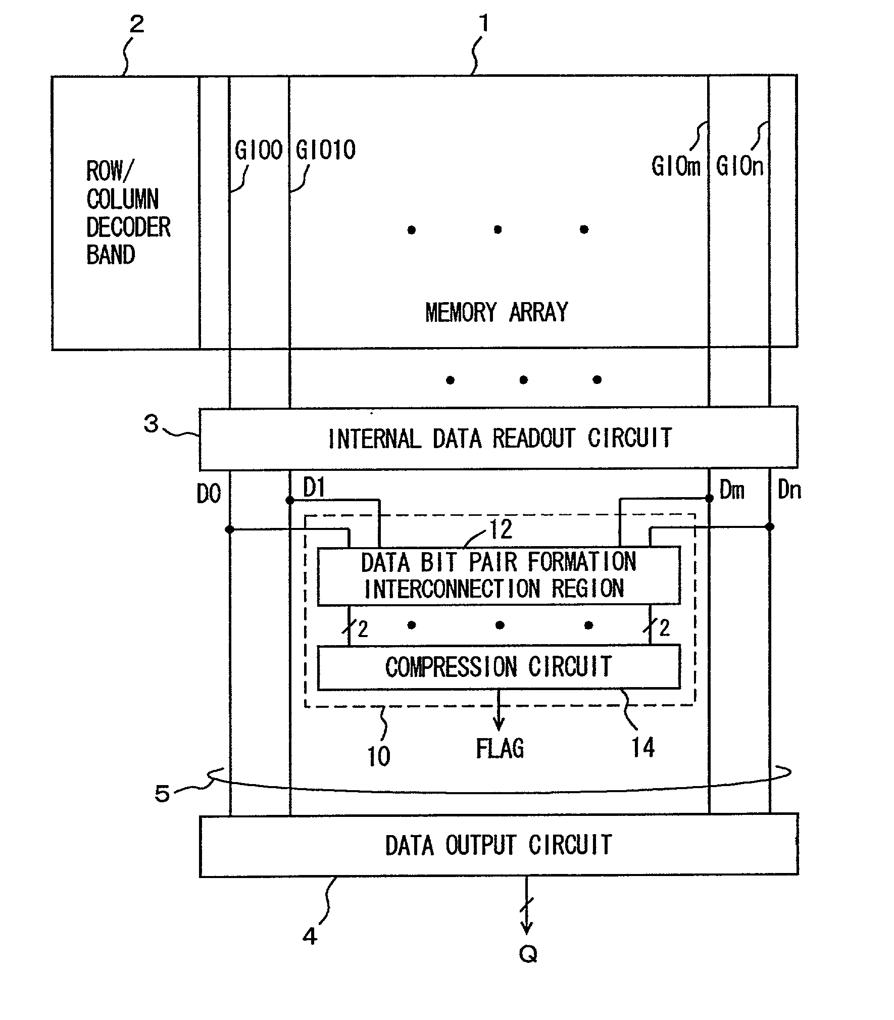
[0031] FIG. 1 is a diagram schematically showing the structure of a main part of the semiconductor memory device according to the present invention. In FIG. 1, the semiconductor memory device includes a memory array 1 having a plurality of memory cells arranged in rows and columns, and a row / column decoder band 2 for selecting a row of and a column of the memory cells in memory array 1. In row / column decoder band 2, row decoders for selecting a memory cell row in memory array 1, and column decoders for selecting a memory cell column in memory array 1 are placed in alignment with each other. In memory array 1, word lines arranged corresponding to the memory cell rows, and column selecting lines transmitting a column selection signal for selecting a memory cell column are arranged along the direction of rows.
[0032] Over memory array 1, global data line pairs GIO0-GIOn are arranged to transmit internal data.
[0033] The selected columns of memory array 1 are conn...
second embodiment
[0041] [Second Embodiment]
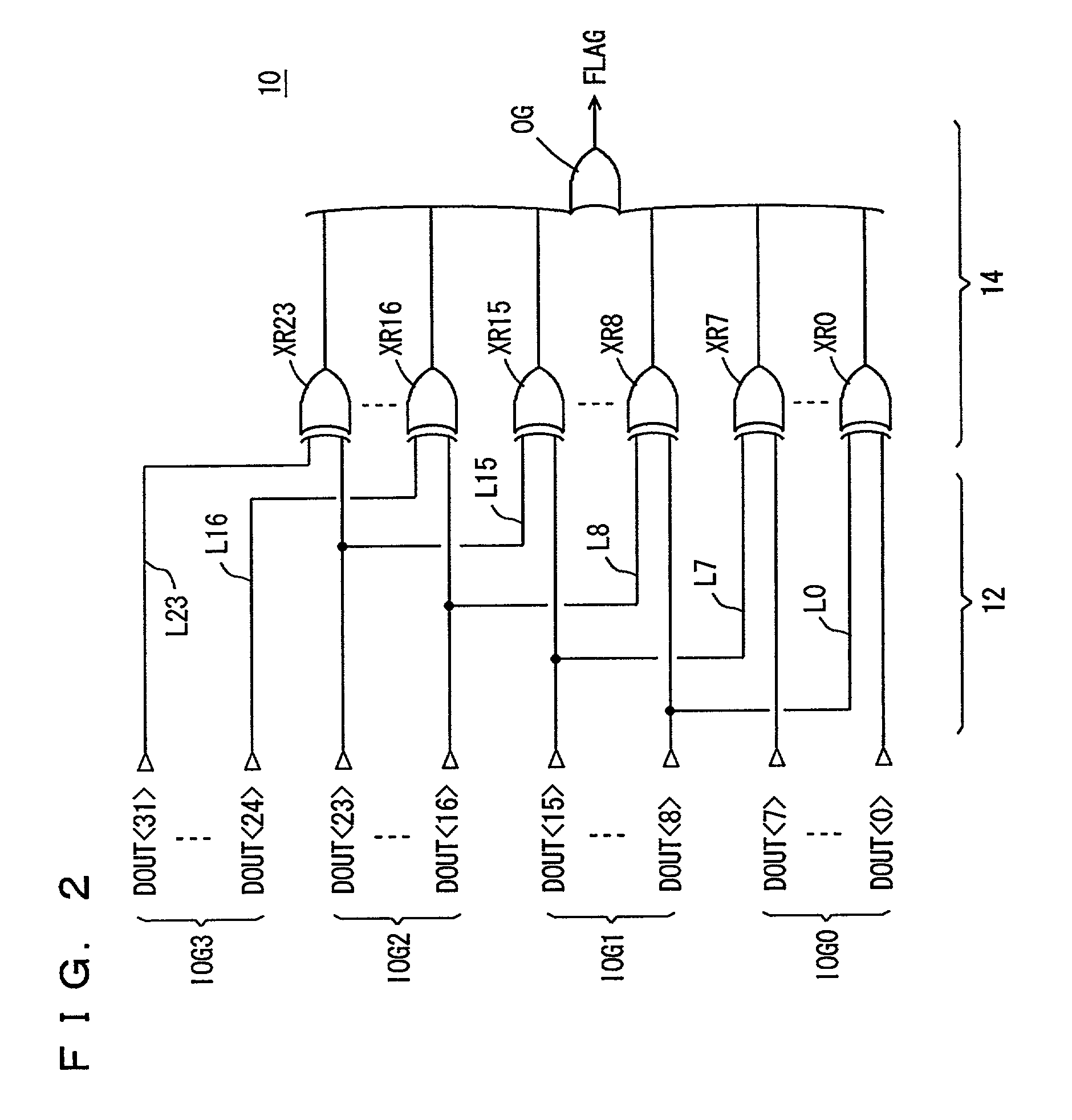
[0042] FIG. 2 shows the structure of multi-bit test circuit 10 according to the second embodiment of the present invention. Multi-bit test circuit 10 shown in FIG. 2 handles 32-bit readout data DOUT-DOUT correspond to data bits D0-Dn or a part of them shown in FIG. 1.
[0043] Data DOUT-DOUT are divided into four data groups IOG0-IOG3 each having 8-bit data. In data bit pair formation interconnection region 12 of multi-bit test circuit 10, internal interconnection lines L0-L23 are so arranged that data bits in the same positions in adjacent data groups make pairs. For example, as shown in FIG. 2, internal interconnection line L0 is so arranged that data bit DOUT having the smallest number in data group IOG0 is paired up with readout data bit DOUT having the smallest number in adjacent data group IOG1. Internal interconnection line L7 pairs up internal readout data bit DOUT with readout data bit DOUT in adjacent data group IOG1.
[0044] In data group IOG1, intern...
third embodiment
[0052] [Third Embodiment]
[0053] FIG. 3 schematically shows the structure of multi-bit test circuit 10 according to the third embodiment of the present invention. In multi-bit test circuit 10 shown in FIG. 3, EXOR gates XR24-XR31 are provided corresponding to readout data bits DOUT-DOUT- , respectively, in addition to the structure of multi-bit test circuit 10 shown in FIG. 2. As the teacher data bits for readout data bits DOUT-DOUT, readout data bits DOUT-DOUT<7&- gt; in data group IOG0 adjacent in the cyclic manner are transmitted to EXOR gates XR24-XR31 via internal interconnection lines L24-L31, respectively.
[0054] The output signals of EXOR circuits XR0-XR31 are applied to OR circuit OGA so as to be compressed finally to 1-bit flag FLAG.
[0055] The relation between data bits DOUT and the teacher data is the same as in the second embodiment, so that the corresponding components are referred to with the same reference numerals, and their detailed description will be omitted.
[0056] ...
PUM
 Abstract
Description
Claims
Application Information