Method for improved plasma nitridation of ultra thin gate dielectrics

a gate dielectric and ultra-thin technology, applied in the field of semiconductor processing, can solve the problems of inability to accept the thickness of the gate dielectric, affecting the overall uniformity of the film thickness, and the non-uniform distribution of nitrogen atoms therein

Inactive Publication Date: 2002-09-19
IBM CORP
View PDF15 Cites 35 Cited by
  • Summary
  • Abstract
  • Description
  • Claims
  • Application Information

AI Technical Summary

Benefits of technology

0005] The above discussed and other drawbacks and deficiencies of the prior art are overcome or alleviated by a method for forming a gate dielectric for an integrated circuit device. In an exemplary embodiment of the invention, the method includes forming an initial oxynitride layer upon a substrate material, the oxynitride layer having an initial physical thickness. The initial oxynitrid

Problems solved by technology

However, there are several associated drawbacks with conventional methods of plasma nitridation used in conjunction with gate thicknesses around 15 .ANG. or less.
This may result in unacceptable gate dielectric thicknesses where it desired to maintain the physical thickness around 15-20 .ANG.. In addition, the direct nitridation of a silicon oxide layer typically results in a non-uniform distribution of nitrogen atoms therew

Method used


Image

  • Method for improved plasma nitridation of ultra thin gate dielectrics
  • Method for improved plasma nitridation of ultra thin gate dielectrics
  • Method for improved plasma nitridation of ultra thin gate dielectrics

Examples


Embodiment Construction

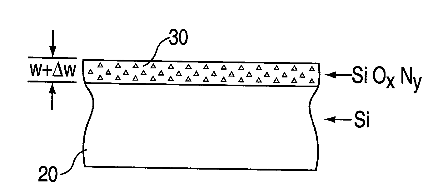
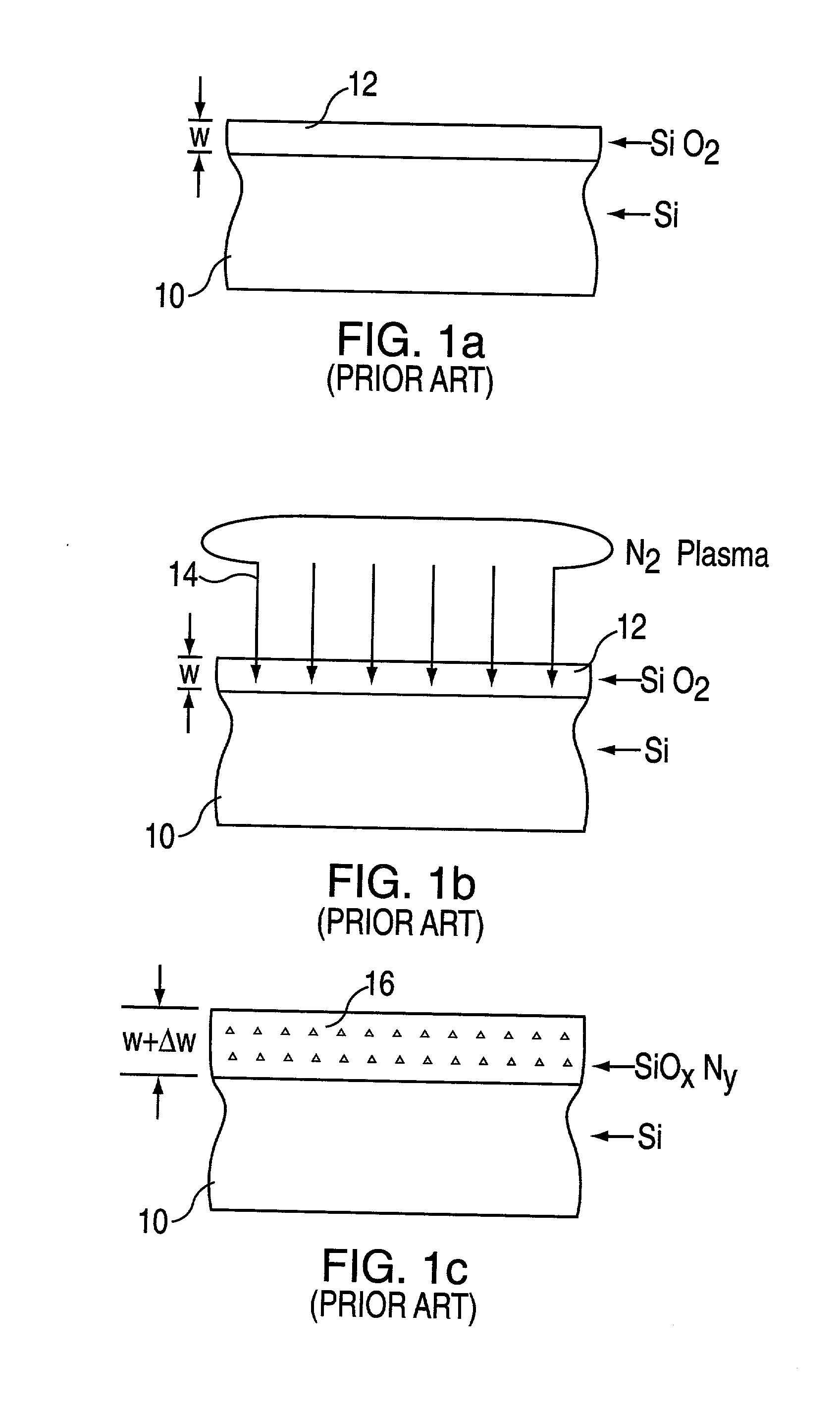
[0016] Referring initially to FIGS. 1(a) through 1(c), a known process of nitriding a gate oxide layer is illustrated. First, a silicon substrate 10 is subjected to oxidation, such as by heating the substrate 10 in a oxygenated environment, thereby forming an insulating oxide layer 12 of SiO.sub.2. As discussed previously, the dielectric performance of the oxide layer 12 becomes increasingly important as gate thicknesses shrink into the deep sub-micron dimensions. In order to improve the dielectric constant of the oxide layer 12 to achieve lower leakage current per unit capacitance, excited nitrogen atoms are introduced into the oxide layer by a process known as Remote Plasma Nitridation (RPN), represented by lines 14 in FIG. 1(b). As a result of the RPN process, the oxide layer 12 is converted to a silicon oxynitride layer 16 having the general chemical composition SiO.sub.xN.sub.y, as shown in FIG. 1 (c).

[0017] While the oxynitride layer 16 has a higher dielectric constant than th...


PUM


Abstract

A method for forming a gate dielectric for an integrated circuit device. In an exemplary embodiment of the invention, the method includes forming an initial oxynitride layer upon a substrate material, the oxynitride layer having an initial physical thickness. The initial oxynitride layer is then subjected to a plasma nitridation, the plasma nitridation resulting in final oxynitride layer having a final physical thickness.

Description

BACKGROUND[0001] The present invention relates generally to semiconductor processing and, more particularly, to improved techniques for fabricating gate dielectrics.[0002] As integrated circuits have become smaller and more densely packed, so have the dielectric layers of devices such as field effect transistors and capacitors. With the arrival of ULSI (Ultra Large Scale Integrated circuit) technology and gate dielectrics of less than 15 angstroms (.ANG.) in thickness, the reliability of the dielectric material is of increasing importance.[0003] Nitrogen doping, particularly Remote Plasma Nitridation (RPN), is a known technique for increasing the dielectric constant (and hence the unit capacitance) of silicon oxide dielectrics. An increased dielectric constant, .epsilon., helps in reducing the amount of leakage current experienced as compared to an undoped silicon dioxide layer having the same capacitance. However, there are several associated drawbacks with conventional methods of ...

Claims


Application Information

Patent Timeline
IPC IPC(8): H01L21/28H01L21/314H01L21/318H01L21/265H01L29/51H01L29/78
CPCH01L21/28202H01L29/518H01L21/3144H01L21/2822H01L21/02247H01L21/02326H01L21/02337H01L21/0234H01L21/02332
Inventor KHARE, MUKESH V.D'EMIC, CHRISTOPHER P.HWANG, THOMAS T.JAMISON, PAUL C.QUINLIVAN, J. J.WARD, BETH A.
Owner IBM CORP
Why Eureka
Try Eureka