Method of simulating PLL circuit and computer program product therefor
- Summary
- Abstract
- Description
- Claims
- Application Information
AI Technical Summary
Benefits of technology
Problems solved by technology
Method used
Image

Examples
first embodiment
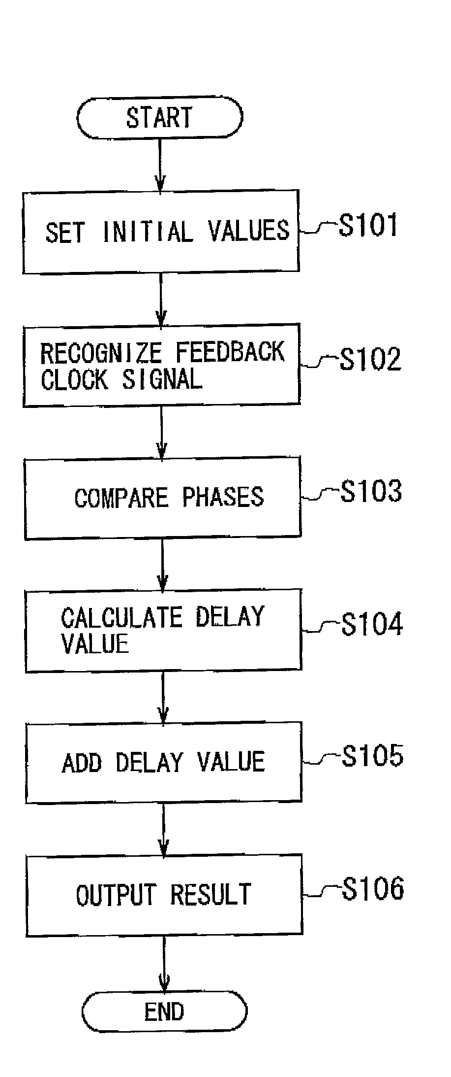
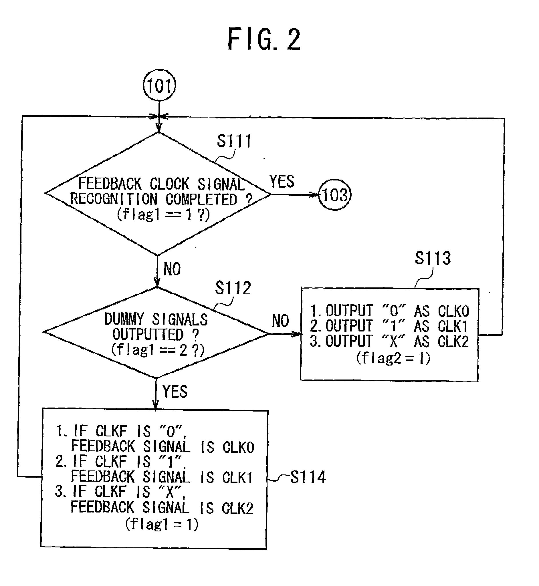
[0065] A method of simulating a PLL circuit according to a first embodiment of the invention is explained below with reference to FIGS. 1 to 4. FIGS. 1 to 3 show the flowcharts of the simulation method of the first embodiment while FIG. 4 shows the configuration of a PLL circuit to which the simulation method is applied.
[0066] As shown in FIG. 4, a PLL circuit 10 comprises a PLL element 11 and a CTS buffer circuit 18. The PLL element 11 has a reference input terminal 12, a fourfold multiplication output terminal 13, a twofold multiplication output terminal 14, a unity-fold multiplication output terminal 15, a lock terminal 16, and a feedback input terminal 17.
[0067] The reference input terminal 12 is used to receive a reference clock signal RCLK with a reference clock frequency of f.sub.R. The fourfold multiplication output terminal 13 is used to output a fourfold multiplication clock signal CLK0 with a fourfold frequency of 4f.sub.R. The twofold multiplication output terminal 14 is...
second embodiment
[0136] A method of simulating a PLL circuit according to.a second embodiment of the invention is explained below with reference to FIGS. 6 and 7. FIG. 6 shows the flowchart of this simulation method while FIG. 7 shows the timing diagram thereof.
[0137] With the simulation method of the first embodiment, the dummy signals having the logic 0, 1, and X are used to recognize the feedback clock signal CLKF. With the simulation method of the second embodiment, unlike this, dummy signals having pulses a, b, and c with different periods or repetition frequencies are used for the same purpose. Since itissufficientto recognize the signal CLKF, the frequencies of the pulses a, b, and c may be set optionally.
[0138] In the step S413 of FIG. 6, the dummy pulsed signals a, b, and c having the different periods or frequencies are outputted to the output terminals 13, 14, and 15, respectively. In other words, the output clock signals CLK0, CLK1, and CLK2 are replaced with the dummy pulsed signals a, ...
third embodiment
[0143] A method of simulating a PLL circuit according to a third embodiment of the invention is explained below with reference to FIGS. 8 and 9. FIG. 8 shows the flowchart of this simulation method while FIG. 9 shows the timing diagram thereof.
[0144] With the simulation method of the third embodiment, dummy signals having different combinations of the logic values "0", "1", and "X" are used. Since it is sufficient to recognize the signal CLKF, the combinations of the values "0", "1", and "X" may be formed optionally.
[0145] In the step S613 of FIG. 9, the dummy pulsed signals having the different combined pulses of "01", "10", and "X1" (2 bits) are outputted to the output clock terminals 13, 14, and 15, respectively. In other words, the output clock signals CLK0, CLK1, and CLK2 are replaced with the dummy signals having the different combinations "01", "10", and "X1", respectively. Then, the value of the "flag 2" is set at "1". Thereafter, the flow is returned to the step S111.
[0146]...
PUM
 Abstract
Description
Claims
Application Information