Pulse output circuit, shift register and display device

Inactive Publication Date: 2002-11-14
SEMICON ENERGY LAB CO LTD
View PDF38 Cites 182 Cited by
  • Summary
  • Abstract
  • Description
  • Claims
  • Application Information

AI Technical Summary

Problems solved by technology

It is difficult, however, to keep a manufacturing cost of the display device down sufficiently in view of a yield.
The number of processes in manufacturing is ideally as few as possible since it directly influence

Method used


Image

  • Pulse output circuit, shift register and display device
  • Pulse output circuit, shift register and display device
  • Pulse output circuit, shift register and display device

Examples


embodiment 1

[0235] An example of producing a display device by means of single conductive TFTs is described in this embodiment.

[0236] The substrate having the pixel TFT and the driver circuit may be manufactured in accordance with a known method, for example, as disclosed in U.S. Pat. No. 5,889,291 issued to Koyama et al. Also, it is possible to crystallize a semiconductor film for an active layer of the TFTs by utilizing a metal element for promoting crystallization although other known methods can be used for crystallization. Such a method of using the metal element is disclosed, for example, in U.S. Pat. No. 5,643,826 issued to Ohtani et al. The entire disclosures of these U.S. Pat. Nos. 5,889,291 and 5,643,826 are incorporated herein by reference.

[0237] FIG. 12 is a schematic view of a display device. A source signal line drive circuit 1201, a gate signal line drive circuit 1202 and a pixel portion 1203 are integrated into one on a substrate 1200 to form a display device. A part enclosed by...

embodiment 2

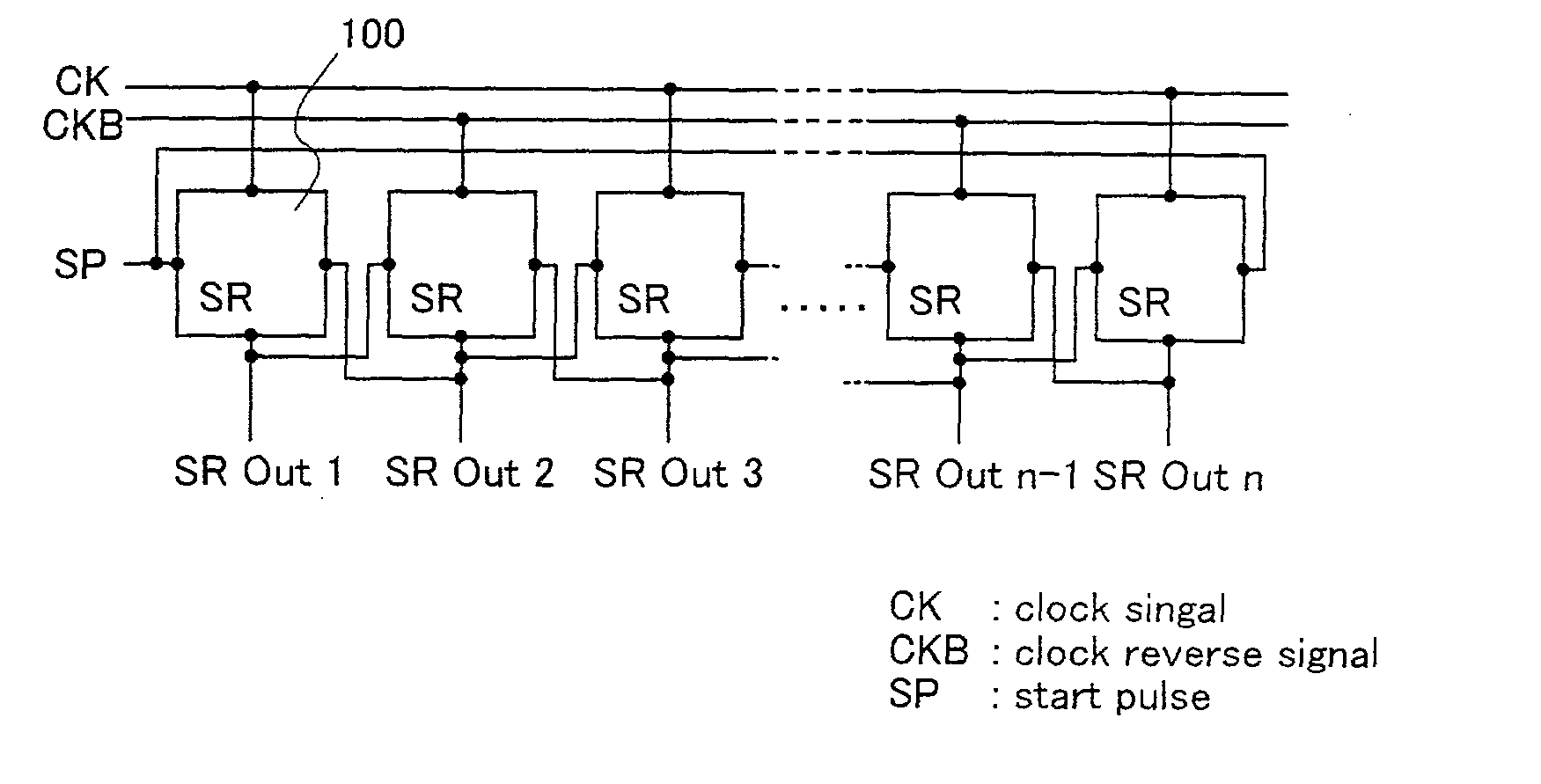
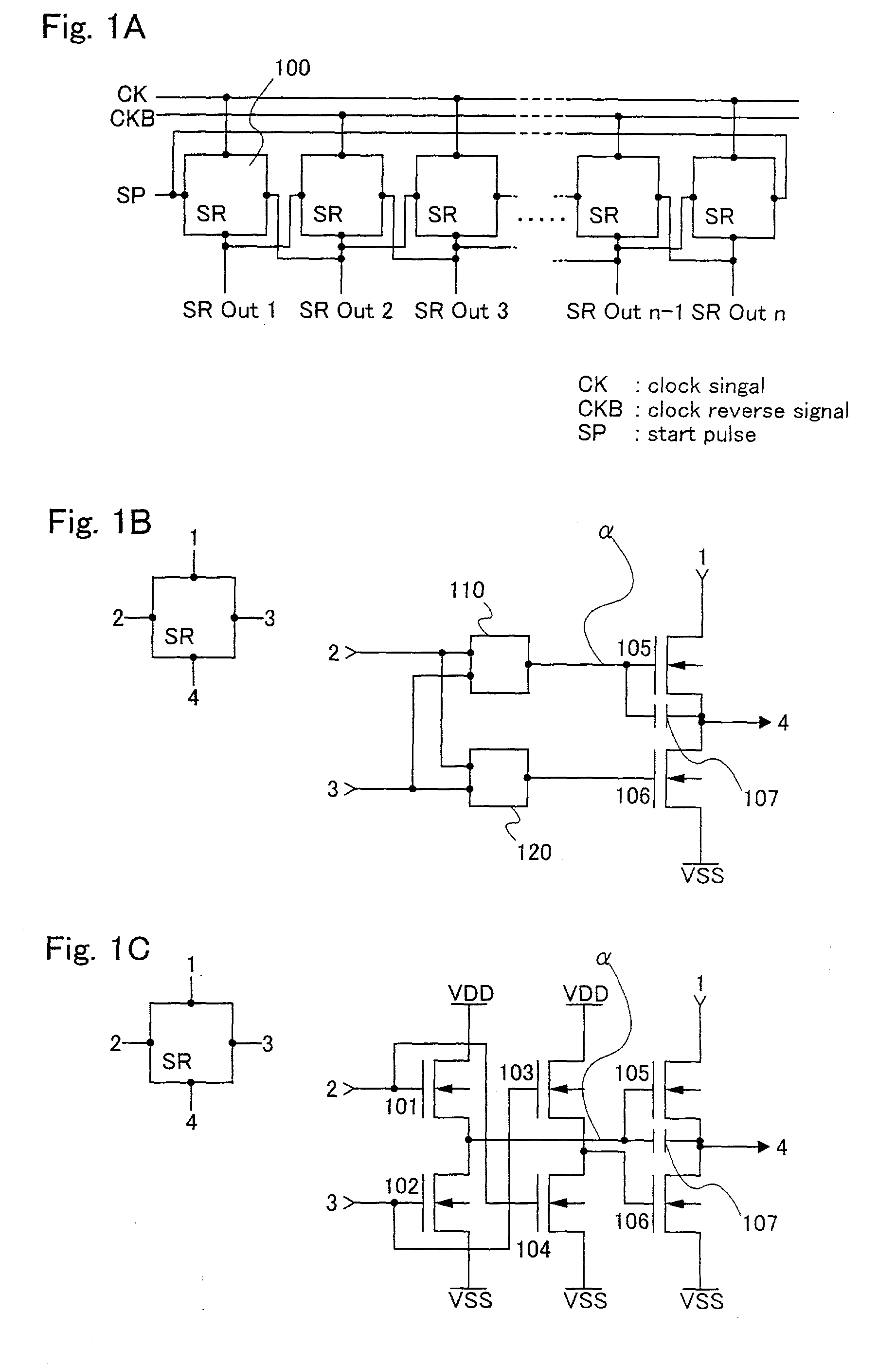
[0258] An example of a simplified structure of the pulse output circuit shown in FIGS. 1A through 1C in the embodiment mode will be described in this embodiment.

[0259] FIGS. 7A through 7C illustrate a shift register of this embodiment. In FIG. 7A, a block 700 is a pulse output circuit for outputting a stage of pulses. The shift register in FIG. 7A comprises n steps of pulse output circuits. FIG. 7B illustrates a detailed circuit structure. A block diagram of the shift register shown in FIG. 1A is same as that of the shift register shown in FIG. 7A and a signal to be inputted is also same in the both cases. This embodiment is different in that a pulse output circuit comprises four TFTs 701 to 704 and a capacity means 705 as shown in FIG. 7C. In FIG. 7B, a block 710 is an amplitude compensation circuit. FIG. 7C illustrated a further detail. In FIG. 7C, the amplitude compensation circuit comprises the TFT 701 connected to the power supply VDD and the TFT 702 connected to the power supp...

embodiment 3

[0265] Refer to FIG. 13 now. In the shift register shown in the embodiment modes 1 and 2 and in the embodiment 2 of the invention, a period of the level H 1301 and that of the level L 1302 of a CK are same in length as shown in FIG. 13A, while a pulse having an opposite polarity to the CK is inputted as a CKB. The width of a sampling pulse is here equal to that of pulses of the CK and the CKB, and thus, an output of the sampling pulse is such as shown by 1303 to 1307 in FIG. 13A. 1303 denotes a sampling pulse at the first stage; 1304 denotes a sampling pulse at the second stage; and following to the above, 1305 to 1307 denote sampling pulses at the third to fifth stages.

[0266] Input / output signals of the CK and the others have a leading edge in changing from the level L to the level H and a trailing edge in changing from the level H to the level L. This may cause overlap of pulses, which ideally must not appear. The sampling pulses 1303 to 1307 shown in FIG. 13A show that a leading ...


PUM


Abstract

A drive circuit of a display device, which comprise only single conductive TFTs and in which amplitude of an output signal is normal, is provided. A pulse is inputted to TFTs 101 and 104 so that the TFTs would turn ON and then potential of a node á rises. When the potential of the node á reaches (VDD-VthN), the node á became in a floating state. Accordingly, a TFT 105 then turns ON, and potential of an output node rises as a clock signal reaches the level H. On the other hand, potential of a gate electrode of the TFT 105 further rises due to an operation of capacitance 107 as the potential of the output node rises, so that the potential of the output node would be higher than (VDD+VthN). Thus, the potential of the output node rises to VDD without voltage drop caused by a threshold of the TFT 105. An output at the subsequent stage is then inputted to TFTs 102 and 103 to turn the TFTs 102 and 103 ON, while the potential of the node á drops down to turn the TFT 105 OFF. A TFT 106 turns ON at the same time so that the potential of the output node would reach the level L.

Description

[0001] 1. Field of the Invention[0002] The present invention relates to a pulse output circuit, a shift register and a display device. In this specification, it is defined that a display device includes a liquid crystal display device in which liquid crystal elements are used as pixels and a spontaneous luminous display device in which spontaneous luminous elements such as electro-luminescence (EL) elements are used. It is also defined that a drive circuit of the display device is a circuit for inputting an image signal into a pixel disposed in the display device to carry out a process of displaying an image and includes a pulse output circuit such as shift register and inverter and an amplification circuit such as amplifier.[0003] 2. Description of the Related Art[0004] Recently, a display device in which a semiconductor thin film is formed on an insulating material, especially on a glass plate, particularly an active matrix type of display device using a thin film transistor (refe...

Claims


Application Information

Patent Timeline
IPC IPC(8): G02F1/133G09G3/20G09G3/30G09G3/36G11C19/00G11C19/28H03K19/0175
CPCG09G3/3688H01L27/1214G02F1/1333G11C19/28G09G3/36G02F1/13306G09G2310/0286G09G2330/021H01L27/124
Inventor AZAMI, MUNEHIRONAGAO, SHOUTANADA, YOSHIFUMI
Owner SEMICON ENERGY LAB CO LTD
Why Eureka
Try Eureka