

System to enable photolithography on severe structure topologies
- Summary
- Abstract
- Description
- Claims
- Application Information
AI Technical Summary
Benefits of technology
Problems solved by technology
Method used
Image

Examples
Embodiment Construction
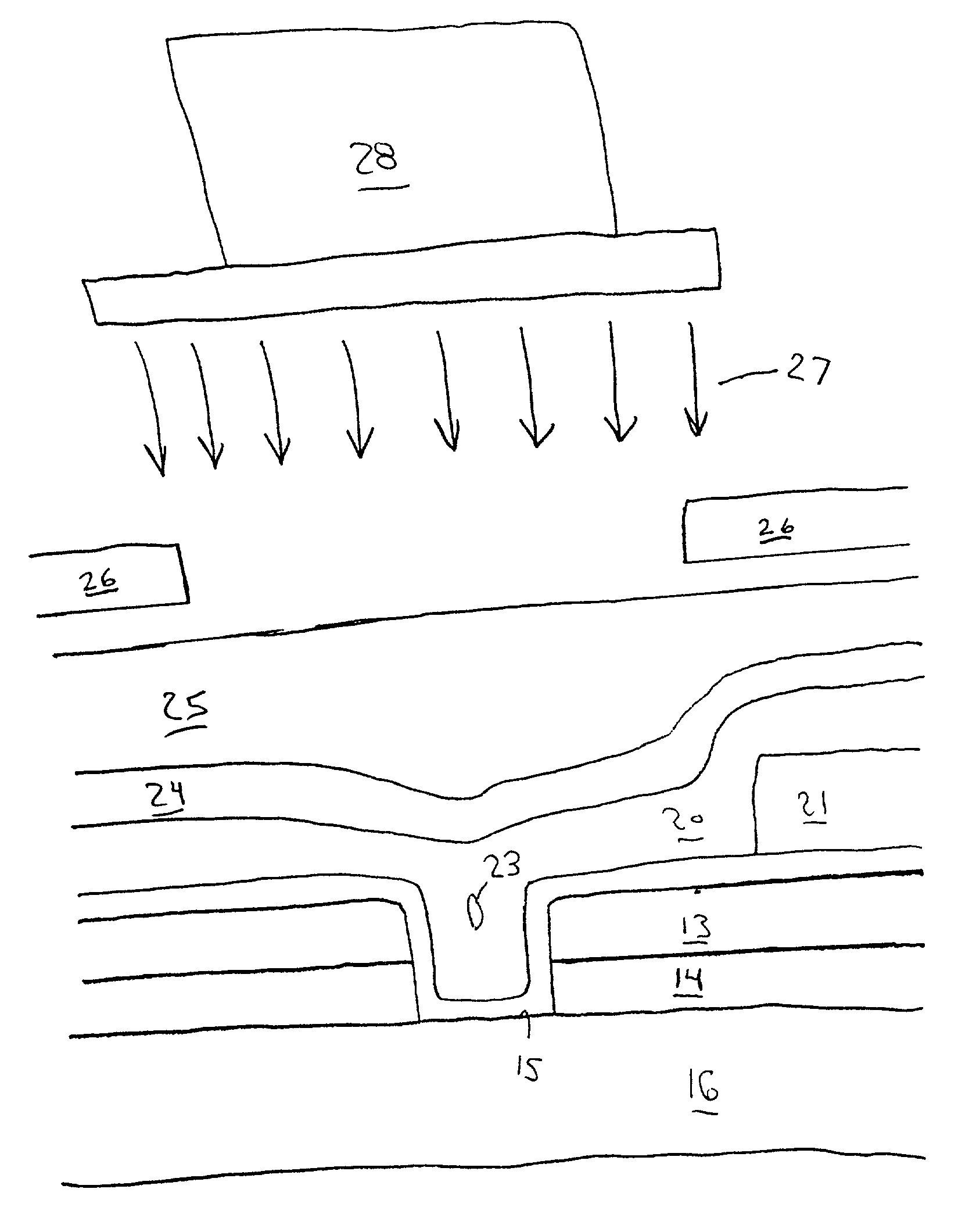
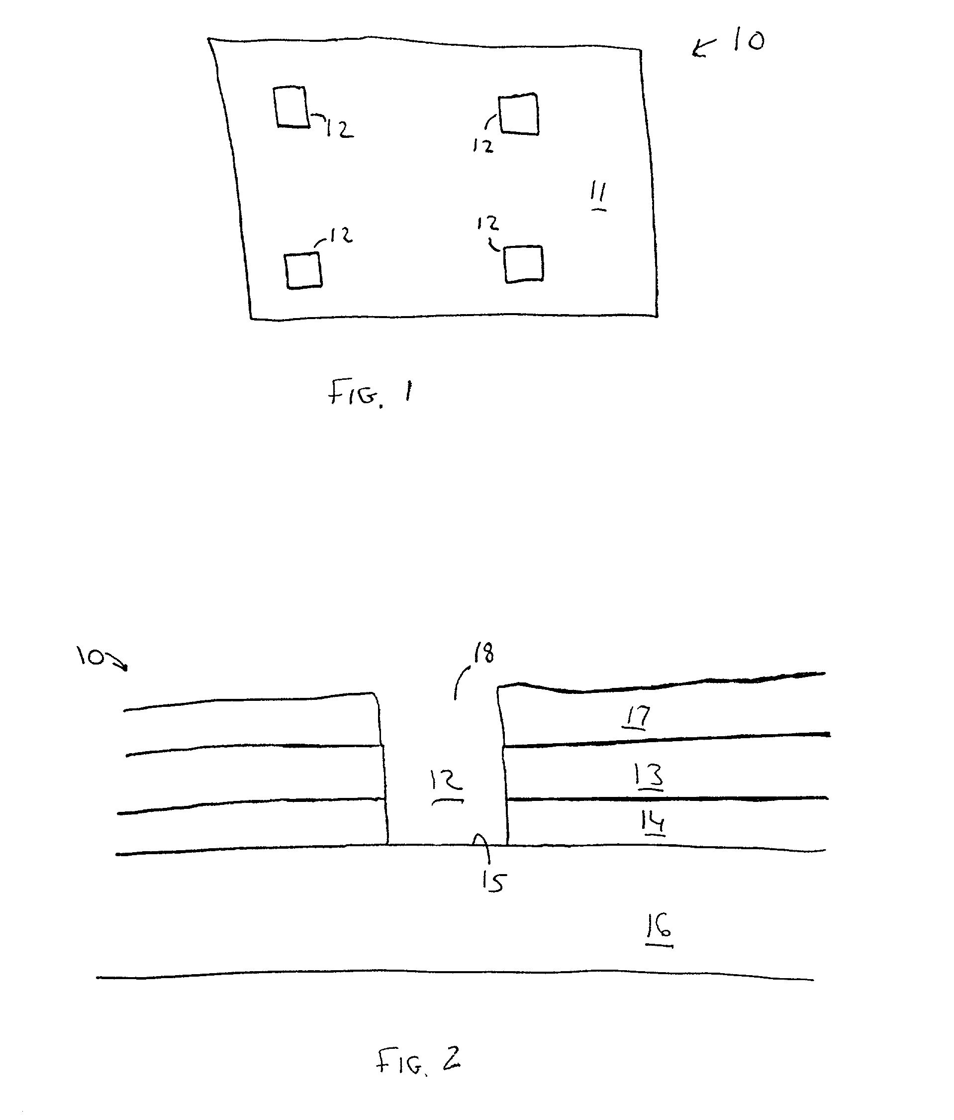
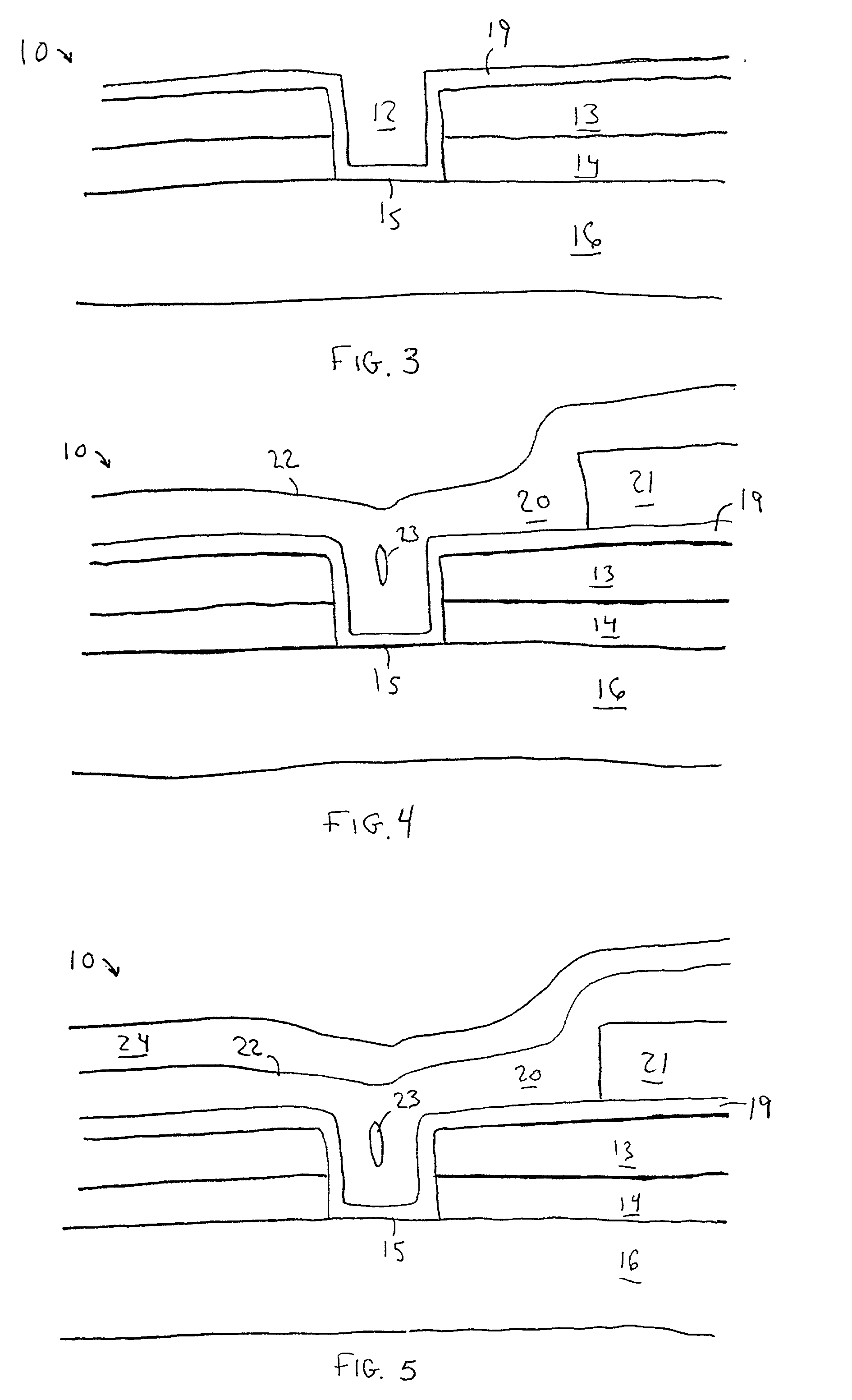
[0022] The present invention is a system and related process steps to substantially reduce, if not eliminate excess photoresist film thickness, and substantially reduce Depth of Focus (DOF) requirements, that would otherwise compromise photolithographic processing. In particular, the present invention resolves unworkable lithography pattern feature size control associated with extreme film thickness variations combined with stepper focus requirements. Specifically, relatively deep contours, holes, cavities, and the like are closed up using a conformal film deposition to reduce their depth and thereby reduce the photoresist film thickness variations such that control of feature sizes of a topographical semiconductor wafer is restored. While a particular embodiment of the present invention is described herein in relation to a semiconductor fabrication process, it is not limited thereto. Instead, it is suitable for any small-scale fabrication process in which severe topologies are pres...
PUM
| Property | Measurement | Unit |
|---|---|---|
| Thickness | aaaaa | aaaaa |
| Structure | aaaaa | aaaaa |
| Electrical conductor | aaaaa | aaaaa |
Abstract
Description
Claims
Application Information