
Method and system for wafer and device-level testing of an integrated circuit

a technology of integrated circuits and test methods, applied in the direction of testing circuits, resistance/reactance/impedence, instruments, etc., can solve the problems of circuit card faults circuit card faults, etc., and achieve the effect of reducing the number of test equipmen

Inactive Publication Date: 2002-11-21
MCCORD DON
View PDF13 Cites 32 Cited by
  • Summary
  • Abstract
  • Description
  • Claims
  • Application Information

AI Technical Summary

Benefits of technology

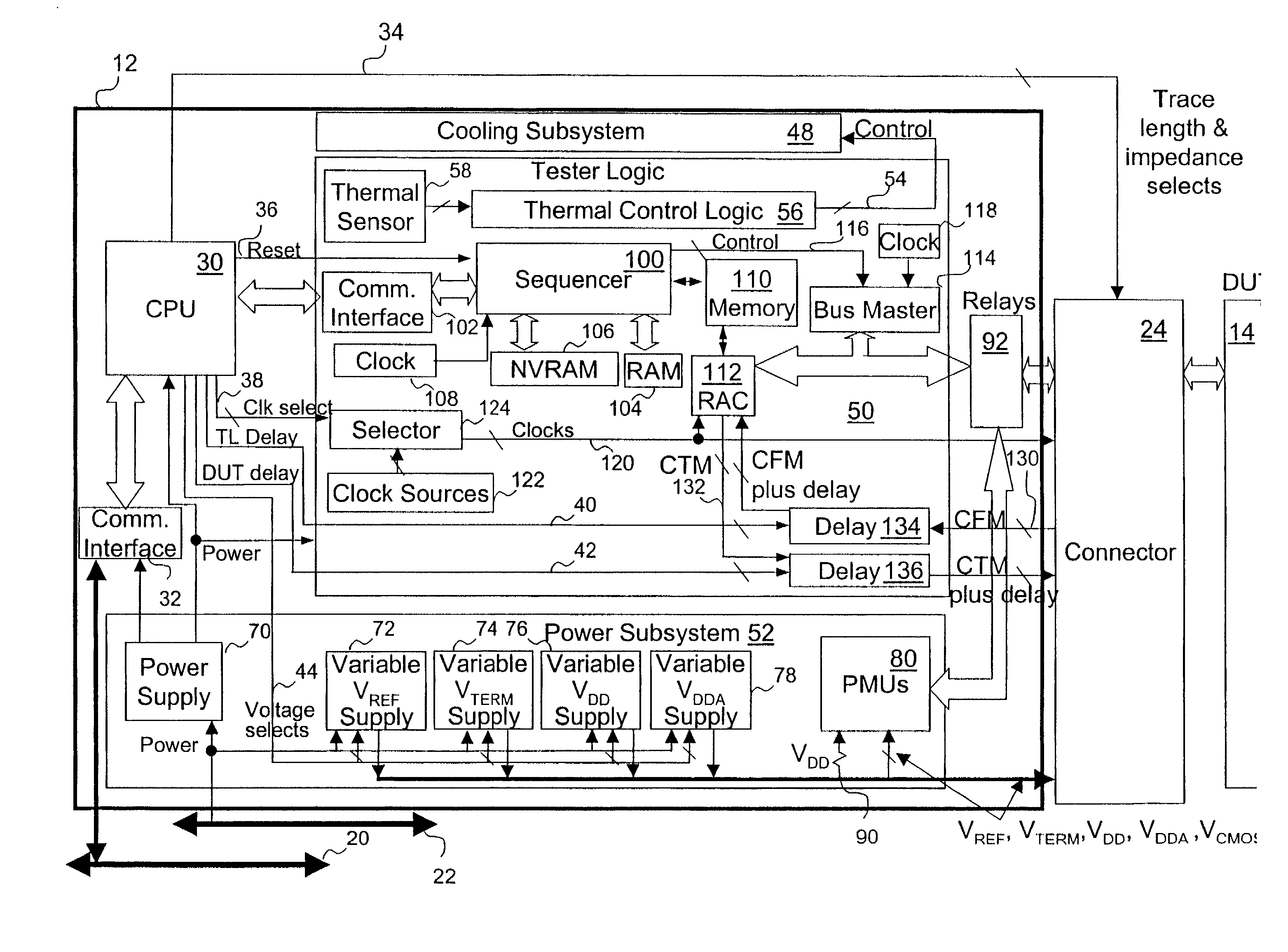
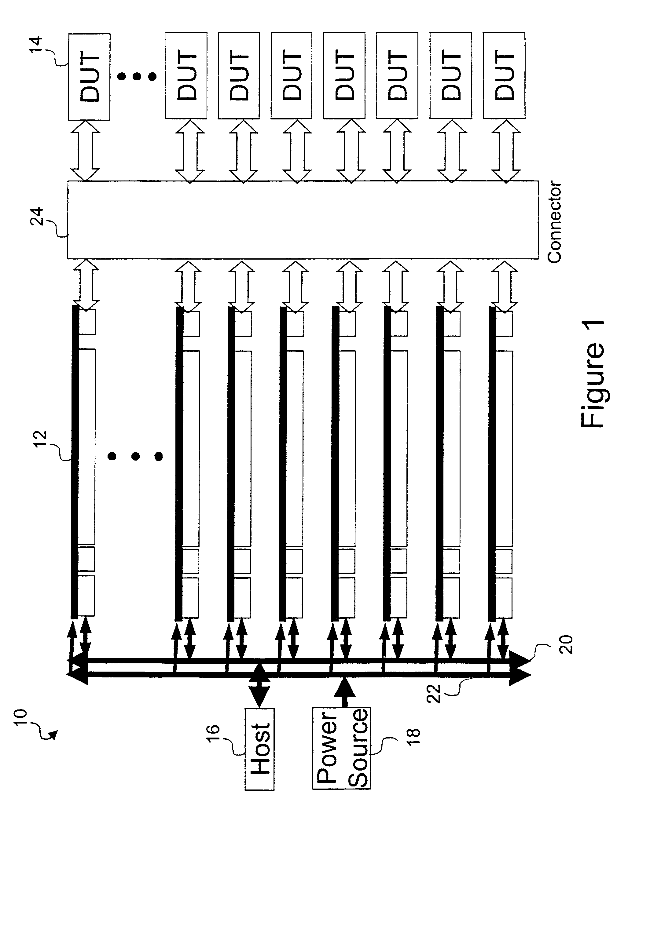
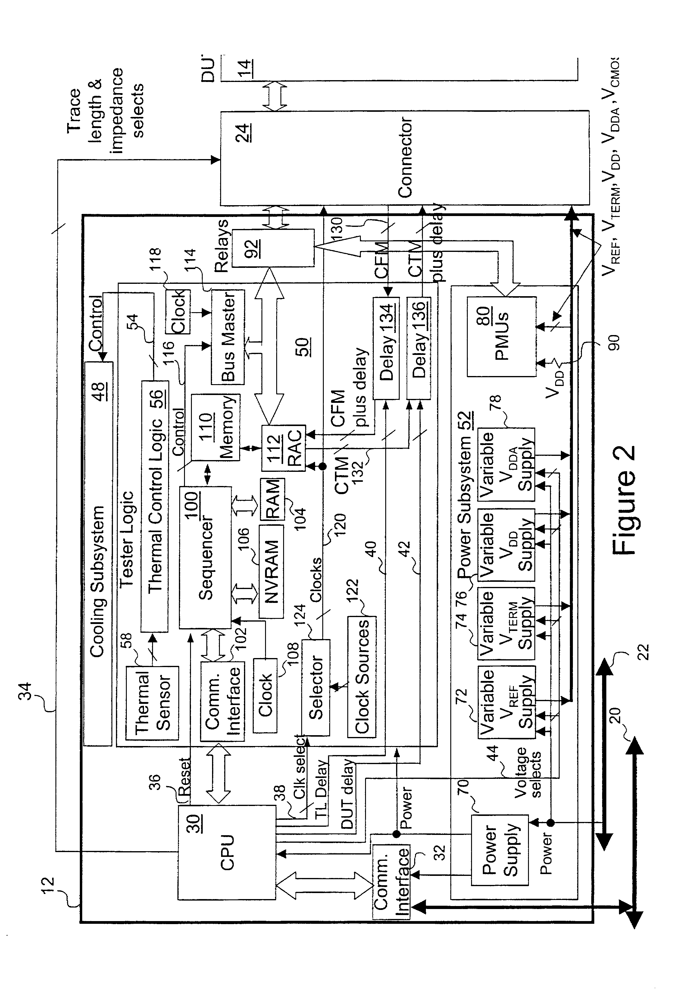
[0014] According to a preferred embodiment of the present invention, a tester comprises test logic and a connector for at least one device under test. The connector, which may comprise a wafer probe for dice on a wafer or a test fixture for packaged integrated circuit devices, has connections for the device under test that present an impedance selected to emulate the characteristic impedance of an end-use environment of the device under test. For example, in an embodiment in which the device under test comprises logic devices using Rambus.TM. Signal Levels to interface to memory and the end-use environment is a Rambus.TM. channel connecting to Rambus DRAMs (RDRAMs), the characteristic impedance is between approximately 20 and 60 ohms. If, on the other hand, the end-use environment is connection to a socket for Rambus.TM. memory modules, then the characteristic impedance is approximately 28 ohms. Alternatively, if the end-use environment is connection to a socket for double data rate (DDR) memory modules, then the characteristic impedance is approximately 60 ohms. Thus, the tester of the present invention can accurately simulate operational behavior in an end-use environment of the device under test. Because this accurate simulation is available even for dice on a wafer, the needless expense associated with packaging defective dice and assembling defective dice onto boards can be avoided.
[0015] The test logic, which is coupled to the connector for communication with the device under test, transfers test commands and test data to the device under test. The test data and commands are utilized to perform multiples types of tests, including tests of the core logic and interface logic of the device under test. In this manner, the need for multiple types of testers is reduced or eliminated.

Problems solved by technology

Device-level testing also differs from wafer probe testing in that device-level testing is typically performed at or near the rated signal frequencies of the external DRAM, and these frequencies often require more sophisticated and expensive test equipment.
Each logic board is then typically subjected to a final, intensive fault test prior to shipping or installation.
The faults detected by board testing include faults in the circuit cards themselves (e.g., open or shorted traces), faults introduced by board assembly (e.g., damaged pin drivers, open or shorted pins, and ESD damage), and undetected faults in the logic device circuitry.
One drawback of the conventional logic device manufacturing process outlined above is that a number of faults are not discovered until late in the manufacturing process, for example, during device-level and board testing.
Unfortunately, the expense of the sophisticated test equipment currently required to fully exercise integrated DRAM interface circuitry prohibits its use during wafer testing.
A second drawback of the conventional manufacturing process is that several different pieces of specialized test equipment are required to fully test many integrated circuit logic devices.
A third drawback of the prior art is that conventional test equipment does not fully emulate the intended end-use environment of devices under test.
This input impedance cannot be adjusted and may result in test behavior that is quite different from the operating behavior of the logic with DRAM interface device under test when it is eventually installed in an end-use environment.
Consequently, there may be an unacceptably high number of faulty devices or boards that pass the test process and even some satisfactory devices that fail the test process.

Method used


Image

  • Method and system for wafer and device-level testing of an integrated circuit
  • Method and system for wafer and device-level testing of an integrated circuit
  • Method and system for wafer and device-level testing of an integrated circuit

Examples


first embodiment

[0099] Referring now to FIG. 11A, there is depicted a high-level block diagram of test fixture embodiment capable of testing a DUT 14 already manufactured onto a circuit board. DUT 14 is able to communicate with a logic tester 250 through connection to an unpopulated device site on the Rambus channel 270. FIG. 11B is a more detailed depiction of an unpopulated device site 270 on the Rambus channel having a plurality of pads, including pad 272. FIG. 11C shows a single finger of a controlled impedance probe 274, which interfaces with connector 24 of logic tester 250 by contacting pad 272. The controlled impedance probe 274 allows DUT 14 to communicate with logic tester 250 via unpopulated device site on the Rambus channel 270 as if DUT 14 was directly connected to the connector 24 of logic tester 250. The test fixture embodiment shown in FIGS. 11A-11C offers the ability to test many functions of system board 252 or peripheral board 264 after DUT 14 is manufactured onto the circuit boa...

second embodiment

[0115] Referring now to FIG. 20A, there is depicted a test fixture for testing DUTs 14 using communication over a DDR memory bus, where the DUTs are manufactured onto circuit boards. As can be seen by comparison of FIG. 20A with FIG. 12A, the two test fixture embodiments are somewhat similar. However, in order to support use of DDR communication in the embodiment of FIG. 19A, there are a number of differences from the RSL embodiment illustrated in FIG. 12A. These differences include replacement of unpopulated Rambus connector 276 with unpopulated DDR connector 298, which may be a socket for a DDR memory module. Fundamental changes to system board 294 and peripheral board 296 that are not essential for an understanding of the present invention make them distinctly different from system board 252 and peripheral board 264 of FIG. 12A. FIG. 20B depicts a more detailed view of the connection of a controlled impedance test fixture 304 within DDR connector 298 of FIG. 20A.

[0116] The presen...


PUM


Abstract

A tester comprises test logic and a connector for at least one device under test. The connector, which may comprise a wafer probe for dice on a wafer or a test fixture for packaged integrated circuit devices, has connections for the device under test that present an impedance selected to emulate the characteristic impedance of an end-use environment of the device under test. For example, in an embodiment in which the device under test comprises Rambus memory and the end-use environment is a Rambus channel, the characteristic impedance is between approximately 20 and 60 ohms. If, on the other hand, the end-use environment is a Rambus memory module, then the characteristic impedance is approximately 28 ohms. Thus, the tester of the present invention can accurately simulate operational behavior in an end-use environment of the device under test. Because this accurate simulation is available even for dice on a wafer, the needless expense associated with packaging defective dies and assembling defective dies into modules can be avoided. The test logic, which is coupled to the connector for communication with the device under test, transfers test commands and test data to the device under test. The test data and commands are utilized to perform multiples types of tests, including tests of the core logic and interface logic of the device under test. In this manner, the need for multiple types of testers is reduced or eliminated.

Description

[0001] 1. Technical Field[0002] The present invention relates in general to testing electronic devices and, in particular, to testing integrated circuits. Still more particularly, the present invention relates to a method and system for wafer and device-level testing of integrated circuits such as logic devices.[0003] 2. Description of the Related Art[0004] Integrated electronic circuits, such as logic devices, are often designed to use external devices, such as dynamic random access memories (DRAMs), to provide data storage in electronic systems, such as computer systems. To ensure proper operation of the electronic systems, the manufacturing process for integrated circuit logic devices includes a number of testing steps intended to verify that the logic devices will provide reliable performance over the expected lifetime of the electronic systems in which they are installed.[0005] A typical manufacturing process for logic devices begins with the fabrication of a semiconductor wafe...

Claims


Application Information

Patent Timeline
Patent Type & Authority Applications(United States)
IPC IPC(8): G01R31/30G01R31/3185G01R31/319G11C29/00G11C29/48G11C29/56
CPCG01R31/30G01R31/3016G01R31/318505G01R31/318511G01R31/31905G11C29/56G01R31/31926G11C7/1066G11C29/006G11C29/48G01R31/31924
Inventor MCCORD, DON
Owner MCCORD DON
Learn More