Method and system for wafer and device level testing of an integrated circuit

a technology of integrated circuits and test methods, applied in the field of electronic devices, can solve the problems of requiring more sophisticated and expensive test equipment, affecting the accuracy of test results, and the failure of circuit cards themselves, so as to reduce the need for multiple types of testers, and avoid the effect of failur

Inactive Publication Date: 2005-08-09
MCCORD DON
View PDF17 Cites 17 Cited by
  • Summary
  • Abstract
  • Description
  • Claims
  • Application Information

AI Technical Summary

Benefits of technology

[0016]According to a preferred embodiment of the present invention, a tester comprises test logic and a connector for at least one device under test. The connector, which may comprise a wafer probe for dice on a wafer or a test fixture for packaged integrated circuit devices, has connections for the device under test that present an impedance selected to emulate the characteristic impedance of an end-use environment of the device under test. For example, in an embodiment in which the device under test comprises DDR memory and the end-use environment is a DDR memory module, the characteristic impedance is between approximately 54 and 66 ohms. Thus, the tester of the present invention can accurately simulate operational behavior in an end-use environment of the device under test. Because this accurate simulation is available even for dice on a wafer, the needless expense associated with packaging defective dies and assembling defective dies into modules can be avoided.
[0017]The test logic, which is coupled to the connector for communication with the device under test, transfers test commands and test data to the device under test. The test data and commands are utilized to perform multiples types of tests, including tests of the core logic and interface logic of the device under test. In this manner, the need for multiple types of testers is reduced or eliminated.

Problems solved by technology

Device-level testing also differs from wafer probe testing in that device-level testing is typically performed at or near the rated signal frequencies of the packaged DRAM, which generally requires more sophisticated and expensive test equipment.
Each memory module is then typically subjected to a final, intensive fault test prior to shipping or installation.
The faults detected by module testing include faults in the circuit cards themselves (e.g., open or shorted traces), faults introduced by module assembly (e.g., damaged pin drivers, open or shorted pins, and ESD damage), and undetected faults in the DRAM circuitry.
One drawback of the conventional DRAM manufacturing process outlined above is that a number of faults are not discovered until late in the manufacturing process, for example, during device-level and module testing.
Unfortunately, the expense of the sophisticated test equipment currently required to fully exercise integrated memory circuitry prohibits its use during wafer testing.
A second drawback of the conventional manufacturing process is that several different pieces of specialized test equipment are required to fully test many integrated circuits.
A third drawback of the prior art is that conventional test equipment does not fully emulate the intended end-use environment of devices under test.
This input impedance cannot be adjusted and may result in test behavior that is quite different from the operating behavior of the DRAM device under test when it is eventually installed in an end-use environment.
Consequently, there may be an unacceptably high number of faulty devices or modules that pass the test process and even some satisfactory devices that fail the test process.

Method used


Image

  • Method and system for wafer and device level testing of an integrated circuit
  • Method and system for wafer and device level testing of an integrated circuit
  • Method and system for wafer and device level testing of an integrated circuit

Examples


Embodiment Construction

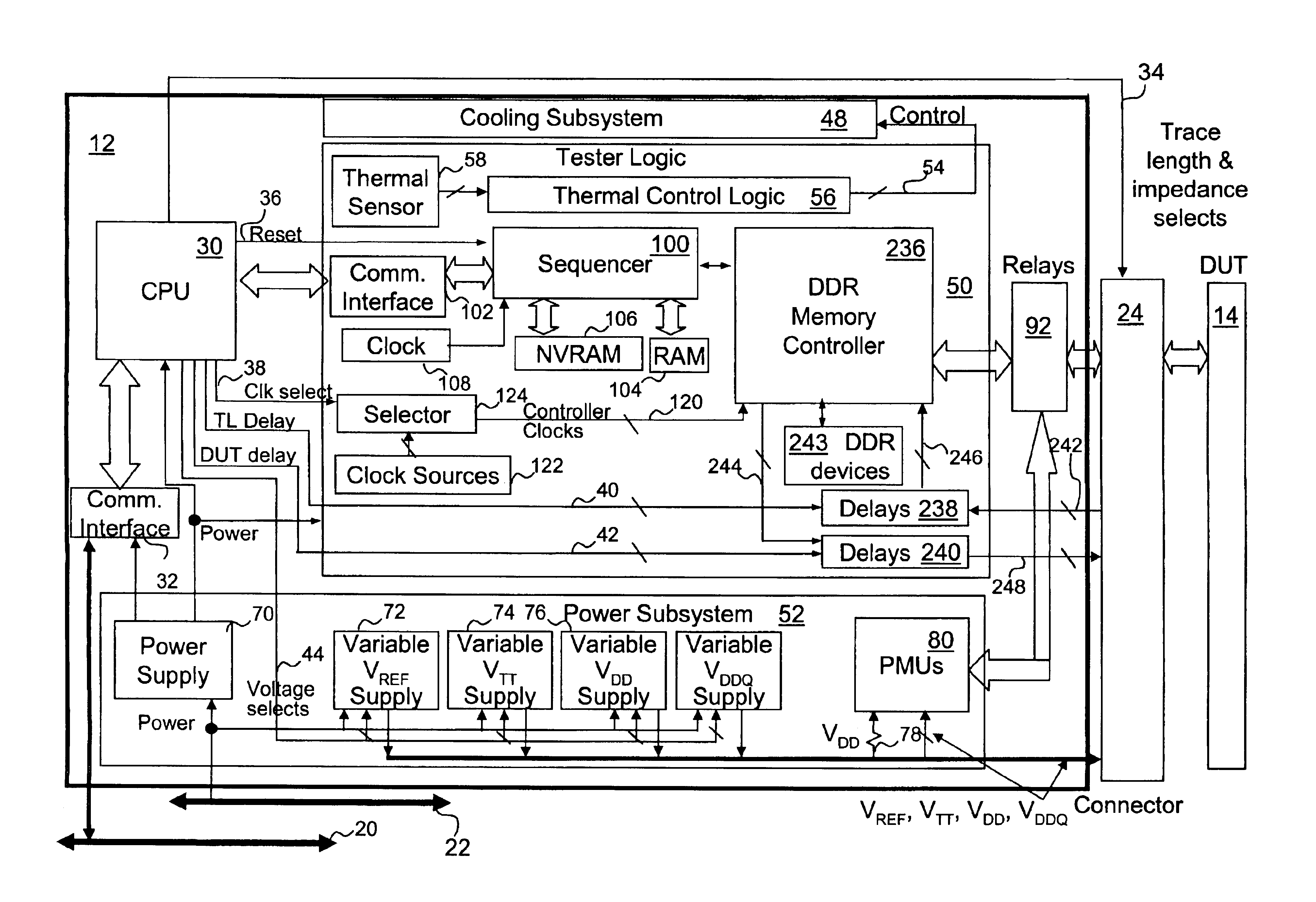
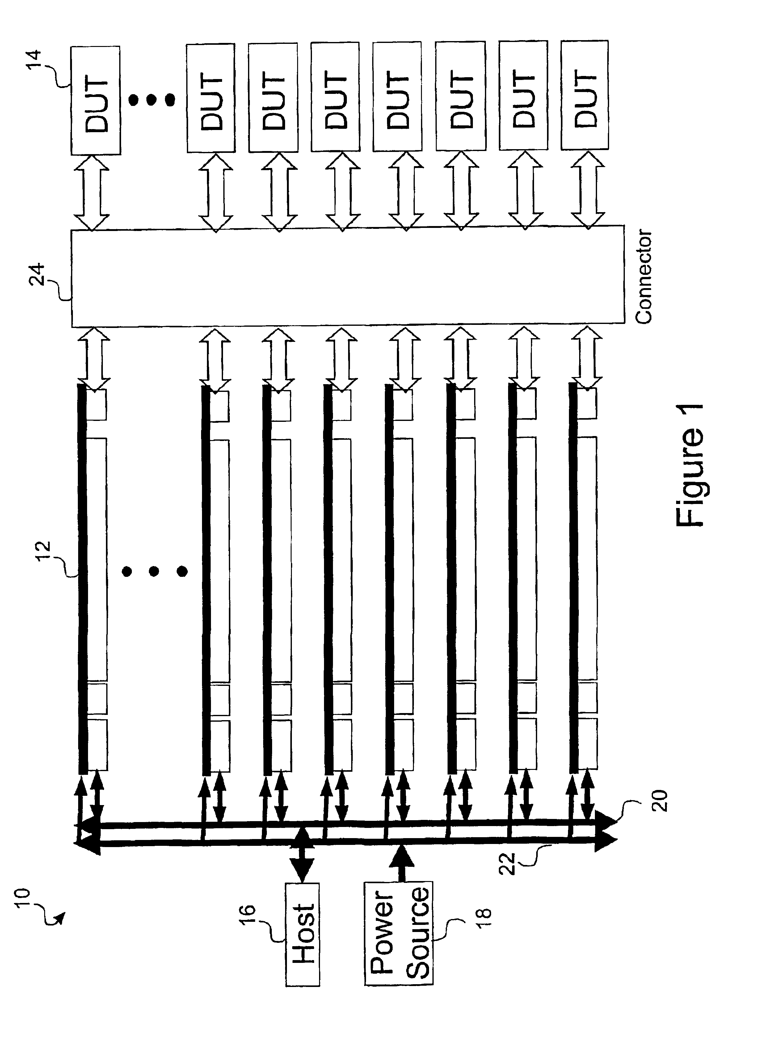
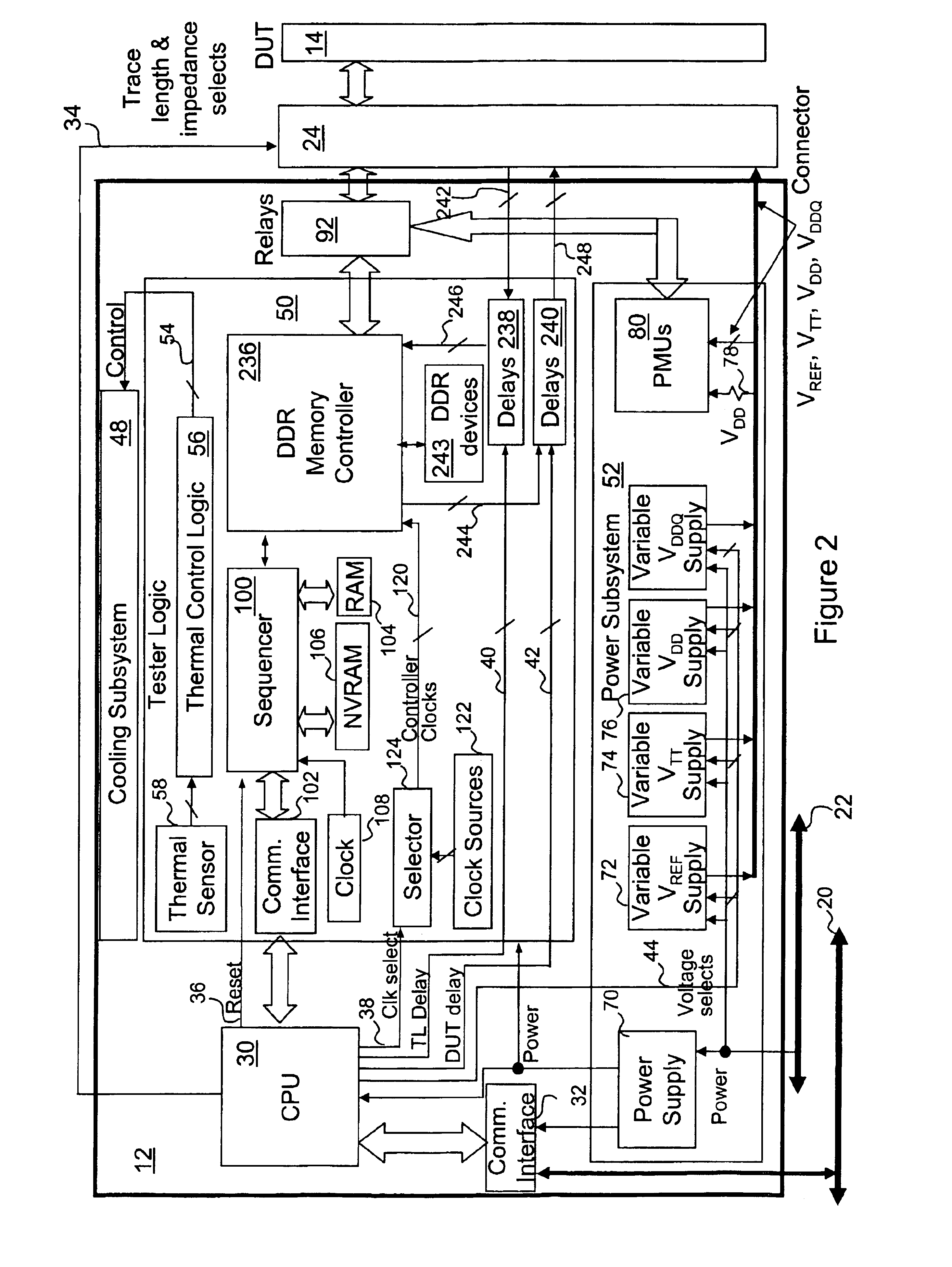
[0037]With reference now to the figures and in particular with reference to FIG. 1, there is depicted a high-level block diagram of an illustrative embodiment of a memory tester in accordance with the present invention. As illustrated, memory tester 10 includes one or more (e.g., 64) tester logic boards 12 that each includes circuitry for testing one device under test 14. In the context of the present invention, a “device under test” (DUT) is defined as either a die on a semiconductor wafer, a packaged integrated circuit device, or a memory module.

[0038]Each tester logic board 12 is coupled to a host 16 and a power source 18 (e.g., 110 V AC) via a communication bus 20 and a power bus 22, respectively. Host 16, which may be a suitably programmed personal computer or a control processor, downloads test procedures and test parameters to and receives test results from tester logic boards 12 via communication bus 20.

[0039]As further illustrated in FIG. 1, each tester logic board 12 is co...


PUM


Abstract

A tester comprises test logic and a connector for at least one device under test. The connector, which may comprise a wafer probe for dice on a wafer or a test fixture or either packaged integrated circuit devices or circuit board modules, has connections for the device under test that present an impedance selected to emulate the characteristic impedance of an end-use environment of the device under test. For example, in an embodiment in which the device under test comprises DDR memory and the end-use environment is a DDR memory module, the characteristic impedance is approximately 60 ohms. Because this accurate simulation is available even for dice on a wafer, the needless expense associated with packaging defective dies and assembling defective dies into modules can be avoided.

Description

[0001]This national stage application claims the benefit of U.S. Provisional Application No. 60 / 234,647, filed on 22 Sep. 2000, and entitled “Method and System for Wafer and Device-Level Testing of an Integrated Circuit.”BACKGROUND OF THE INVENTION[0002]1. Technical Field[0003]The present invention relates in general to testing electronic devices and, in particular, to testing integrated circuits. Still more particularly, the present invention relates to a method and system for wafer and device-level testing of integrated circuits such as memories.[0004]2. Description of the Related Art[0005]Integrated circuit memories, such as dynamic random access memories (DRAMs), are nearly universally utilized to provide data storage in electronic systems, such as computer systems. To ensure proper operation of the electronic systems, the manufacturing process for integrated circuit memories includes a number of testing steps intended to verify that the integrated circuit memories will provide ...

Claims


Application Information

Patent Timeline
Patent Type & Authority Patents(United States)
IPC IPC(8): G11C29/00G11C29/04G11C29/48G11C29/56G01R31/30G01R31/3185G01R31/319
CPCG01R31/318505G01R31/318511G01R31/31905G01R31/31924G01R31/31926G11C7/1066G11C29/006G11C29/48G11C29/56G01R31/30G01R31/3016
Inventor MCCORD, DON
Owner MCCORD DON
Why Eureka
Try Eureka