Conducting material

a technology of conductivity and carbon nanotubes, applied in the field of conductivity materials, can solve problems such as the conductivity of carbon nanotubes

Inactive Publication Date: 2002-12-05
ABB (SCHWEIZ) AG
View PDF4 Cites 24 Cited by
  • Summary
  • Abstract
  • Description
  • Claims
  • Application Information

AI Technical Summary

Problems solved by technology

This is a fundamental limitation for of the carbon nanotube's conductivity and is determined by the number of energy levels that cross the fermi level.
They have a valence electron that is easily donated because of the atom's low ionization energy, however alkali metals are thermally and chemically unstable, they decompose readily and are very hygroscopic.

Method used


Image

  • Conducting material
  • Conducting material
  • Conducting material

Examples


Embodiment Construction

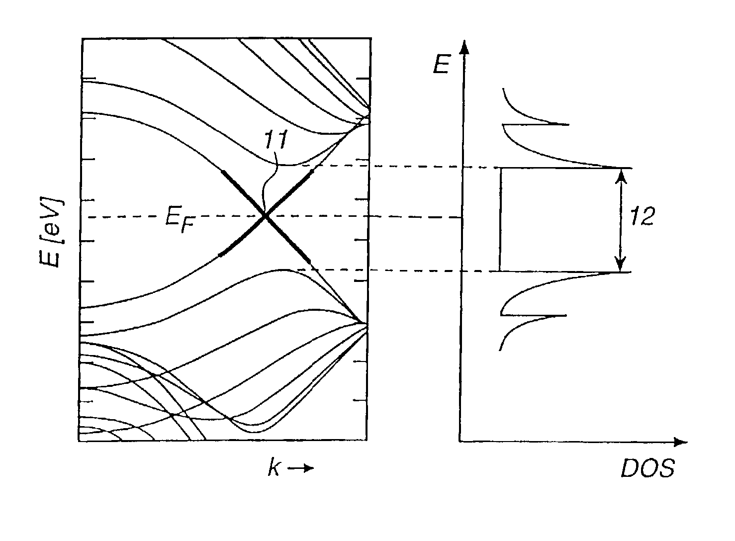
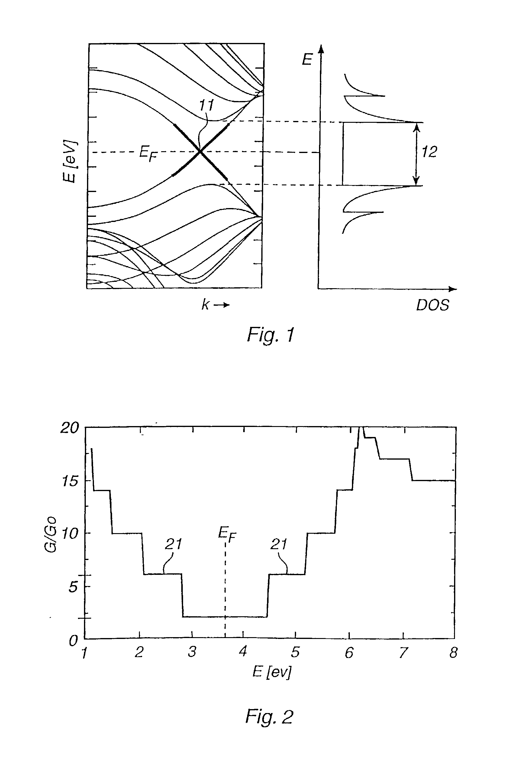
[0037] FIG. 1 shows energy bands and the density of states (DOS) of a metallic (5,5) carbon nanotube, whose fermi energy, E.sub.F, is indicated with a dashed line. Two energy levels cross the fermi energy, 11. The density of states is finite and constant at E.sub.F. The bandgap 12 between the next nearest DOS maximum is about 2 eV.

[0038] FIG. 2 shows a metallic (10,10) carbon nanotube's conductivity as a function of energy. The carbon nanotube's fermi energy, E.sub.F, is 3.65 eV. If current is conducted at the carbon nanotube's fermi energy it's conductivity is 2G.sub.0. If the carbon nanotube's fermi level is shifted up or down so that more energy levels cross the fermi level, the conductivity is enhanced in steps of 4G.sub.0 to 6 G.sub.0, 10 G.sub.0 etc. In order to reach the first step 21, i.e. to increase the conductivity from 2G.sub.0 to 6G.sub.0, the fermi level has to be shifted up or down by about 0.8 eV. Theoretical estimates predict that to attain the necessary shift in th...


PUM

PropertyMeasurementUnit
lengthaaaaaaaaaa
fermi levelaaaaaaaaaa
diameteraaaaaaaaaa

Abstract

Conducting material for an electric conductor comprising nanostructures (31) and a charge-transfer agent that shifts the nanostructures' fermi level so that said nanostructures attain an enhanced conductivity.

Description

[0001] The present invention relates to an electric conductor. More particularly the invention concerns conducting material containing nanostructures having an enhanced electric conductivity.TECHNICAL BACKGROUND[0002] Electrons in an atom can only have certain well-defined energies. The electrons occupy particular energy levels within the atom depending on their energy. Each energy level can accommodate only a limited number of electrons.[0003] If two similar atoms are brought near enough to each other so that they interact, the two-atom system has two adjacent energy levels corresponding to each energy level in the single atom. If ten atoms interact, the ten-atom system has ten energy levels corresponding to each energy level in the individual atom. For solids, the number of atoms and therefore the number of energy levels are very large. A lot of the higher energy levels overlap and merge into regions of allowed energy levels called energy bands. Regions containing no energy levels...

Claims


Application Information

Patent Timeline
Patent Type & Authority Applications(United States)
IPC IPC(8): H01B1/04H01B1/24H01B9/00H02K3/02
CPCB82Y10/00H01B1/04H02K2203/15H01B9/006H02K3/02H01B1/24
Inventor HJORTSTAM, OLOFISBERG, PETER
Owner ABB (SCHWEIZ) AG
Why Eureka
Try Eureka