Data transfer system

a data transfer and data technology, applied in the field of data transfer systems, can solve problems such as reducing performance and lowering the effective data transmission ra

Inactive Publication Date: 2002-12-12
NEC CORP
View PDF6 Cites 51 Cited by
  • Summary
  • Abstract
  • Description
  • Claims
  • Application Information

AI Technical Summary

Problems solved by technology

The above-described large scale system of the prior art was of a system configuration that did not allow a data transfer source to completely verify that data had been written correctly to the ultimate memory device, despite the possibility that erroneous data may be recorded in a memory device due to, for example, the alteration of data to invalid data while being transferred due to the occurrence of an abnormality caused by hardware breakdowns during the data transfer, or due to the occurrence of a parity error caused by elect...

Method used


Image

  • Data transfer system
  • Data transfer system
  • Data transfer system

Examples


first embodiment

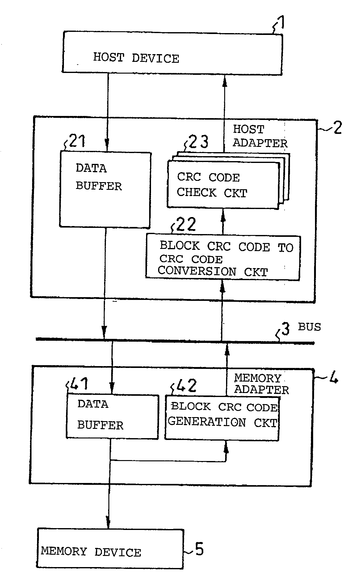
[0053] We refer first to FIG. 1, which is a circuit block diagram showing the configuration of the data transfer system according to the present invention. The principal components of the data transfer system according to this embodiment are constituted by: host device 1 that issues a request to write sector data; host adapter 2 that deblocks the sector data for which a write request has been issued from host device 1 into data block units and that issues a write request to memory adapter 4; system bus 3 that connects host adapter 2 and memory adapter 4; memory adapter 4 that takes in data blocks for which a write request has been issued from host adapter 2, memory-writes the data blocks to memory device 5, generates block CRC code from the data blocks, and returns the block CRC code to host adapter 2 as a write reply; and memory device 5 for memory-writing the data blocks.

[0054] FIG. 1 presents a simplified view of the arrangement in the data transfer between host device 1 and memo...

embodiment 1

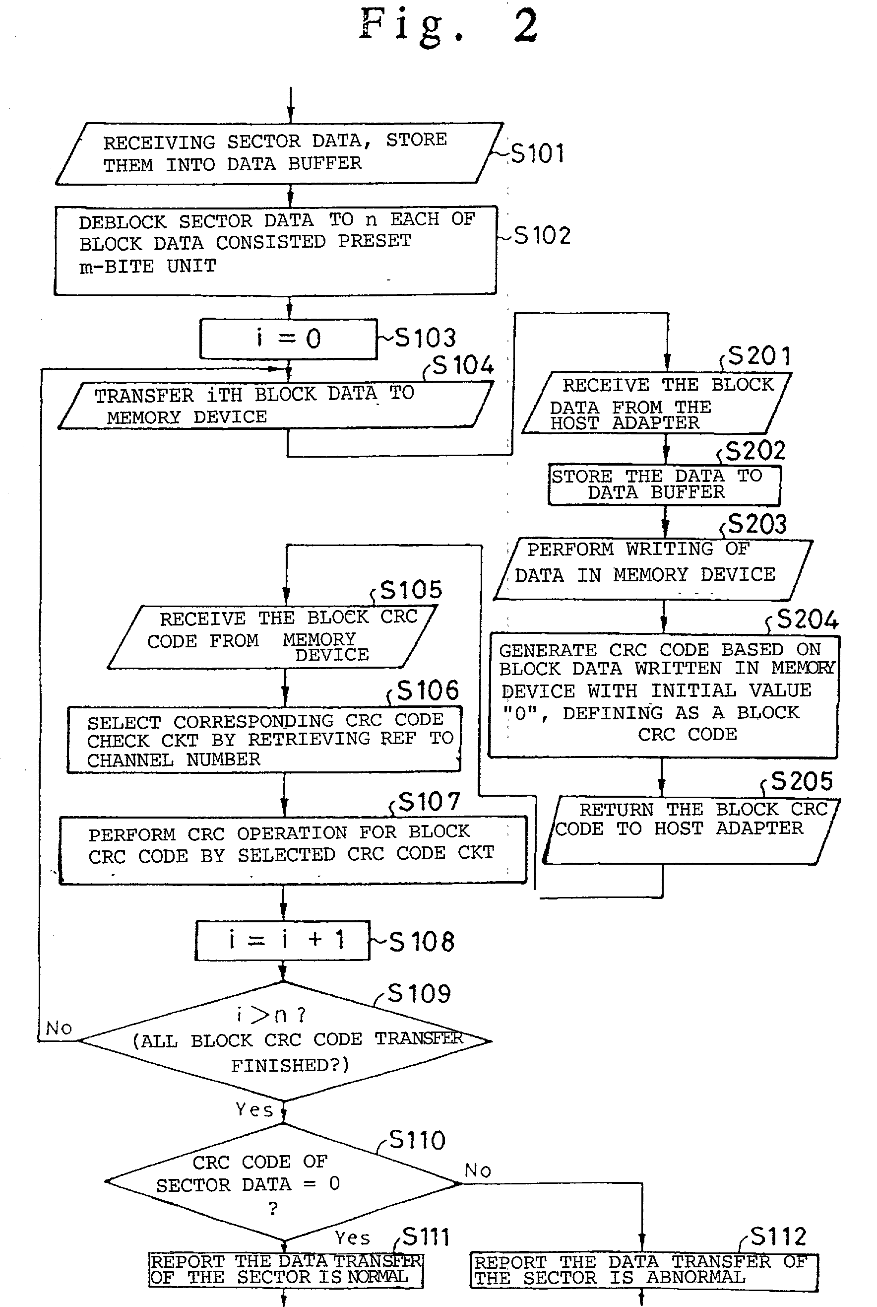
[0067] Simultaneous with the memory-write of the data blocks, memory adapter 4 transfers the data blocks as is to block CRC code generation circuit 42, and block CRC code generation circuit 42 generates CRC code in which initial values are set to zero as block CRC code (Step S204). Details regarding an actual example of the generation of block CRC code by block CRC code generation circuit 42 are next described in embodiment 1 below.

[0068] Memory adapter 4 next returns the generated block CRC code by way of system bus 3 to host adapter 2 as a write reply (Step S205).

[0069] Upon receiving the block CRC code that has been returned as a write reply from memory adapter 4 (Step S105), host adapter 2 uses the block CRC code to CRC code conversion circuit 22 to specify the channel of the data transfer source and select the corresponding CRC code check circuit 23 (Step S106), and then uses the selected CRC code check circuit 23 to perform a CRC computation of the block CRC code that has been...

second embodiment

[0077] We now refer to FIG. 3, in which is shown a circuit block diagram of the configuration of the data transfer system according to the second embodiment of the present invention. The principal components of the data transfer system of this embodiment are constituted by: host devices 1-0-1-p; host adapters 2-0-2-p; request bus 31; reply bus 32; memory adapters 4-0-4-q; and memory devices 5-0-5-q.

[0078] Host adapters 2-0-2-p are constituted to include: data buffers 21-0-21-p, block CRC code to CRC code conversion circuits 22-0-22-p; and CRC code check circuits 23-0-23-p.

[0079] Memory adapters 4-0-4-p are constituted to include: data buffers 41-0-41-q and block CRC code generation circuits 42-0-42-q.

[0080] The operation of the data transfer system according to the second embodiment that is constructed according to the foregoing description is substantially the same as the data transfer system according to the first embodiment shown in FIG. 1, and despite the plurality of memory dev...


PUM


Abstract

A device is disclosed that allows a host device that is the source of data transfer to detect whether or not data have been correctly written to a memory device without interfering with the effective data transfer. When the host device issues a request to write sector data, a host adapter deblocks the sector data into data blocks and transfers the data in data block units to a memory adapter. The memory adapter not only memory-writes the data blocks to a memory device, but also generates block CRC code from the data blocks and returns the code as a write reply to the host adapter. The host adapter receives the block CRC code, carries out a CRC operation to reconstruct CRC code of complete sector data, performs a correspondence check with the CRC code of the original sector data, and reports the check results to the host device.

Description

[0001] 1. Field of the Invention[0002] The present invention relates to a data transfer system, and in particular, to a data transfer system that performs a data check.[0003] 2. Description of the Related Art[0004] If a device that is the source of a data transfer and a device that performs a memory write of data to a memory device are in the same LSI (Large-Scale Integrated Circuit), it is possible to detect whether the data has been reliably written, and it is also easy to detect an abnormal state of the device such as altered data.[0005] In a large-scale system such as a large-scale disk array device, however, the data is not necessarily processed in a single LSI, and writing to a target memory device may be realized by way of various types of buses within the system such as PCI (Peripheral Component Interconnect) buses, and system buses as well as the plurality of LSIs that control these buses.[0006] The above-described large scale system of the prior art was of a system configu...

Claims


Application Information

Patent Timeline
IPC IPC(8): G06F11/10G06F3/06G06F12/16G11B20/10G11B20/18H03M13/00H03M13/09H04L1/00
CPCG06F3/0619G06F3/0656G11B20/18G06F11/1004G11B20/10G06F3/0689
Inventor KOBAYASHI, EIJI
Owner NEC CORP
Why Eureka
Try Eureka