Delay compensation circuit including a feedback loop

a compensation circuit and feedback loop technology, applied in the direction of pulse automatic control, pulse technique, pulse manipulation, etc., can solve the problems of clock signal arriving earlier than expected, data signal violating setup time, other types of synchronous logic elements,

Inactive Publication Date: 2003-01-02
LUCENT TECH INC
View PDF4 Cites 66 Cited by
  • Summary
  • Abstract
  • Description
  • Claims
  • Application Information

AI Technical Summary

Problems solved by technology

For instance, clock skew (i.e., minor variations in the time at which clock signals arrive at their destinations in a chip) may cause the clock signal to arrive earlier than expected.
Therefore, clock skew may cause a data signal to violate the setup time.
Such changes in delay time T.sub.d may result in a violation of the setup time or the hold time of the D flip-flop DFF, or other types of synchronous logic elements.
However, a problem may arise when using the variable control system 100.
Such a problem can be attributed to variations in PVT conditions, and may cause the delay times of the coarse delay and fine delay elements of the tapped delay circuits 10 to vary from below -50% to above 100% of the normal delay time.
Alternatively, the above problem may cause the edge of signal P_CK to fall within time interval S2.

Method used


Image

  • Delay compensation circuit including a feedback loop
  • Delay compensation circuit including a feedback loop
  • Delay compensation circuit including a feedback loop

Examples


Embodiment Construction

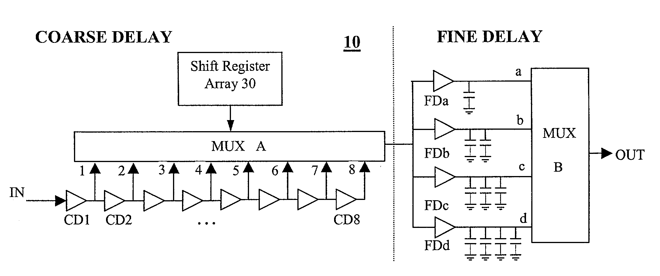
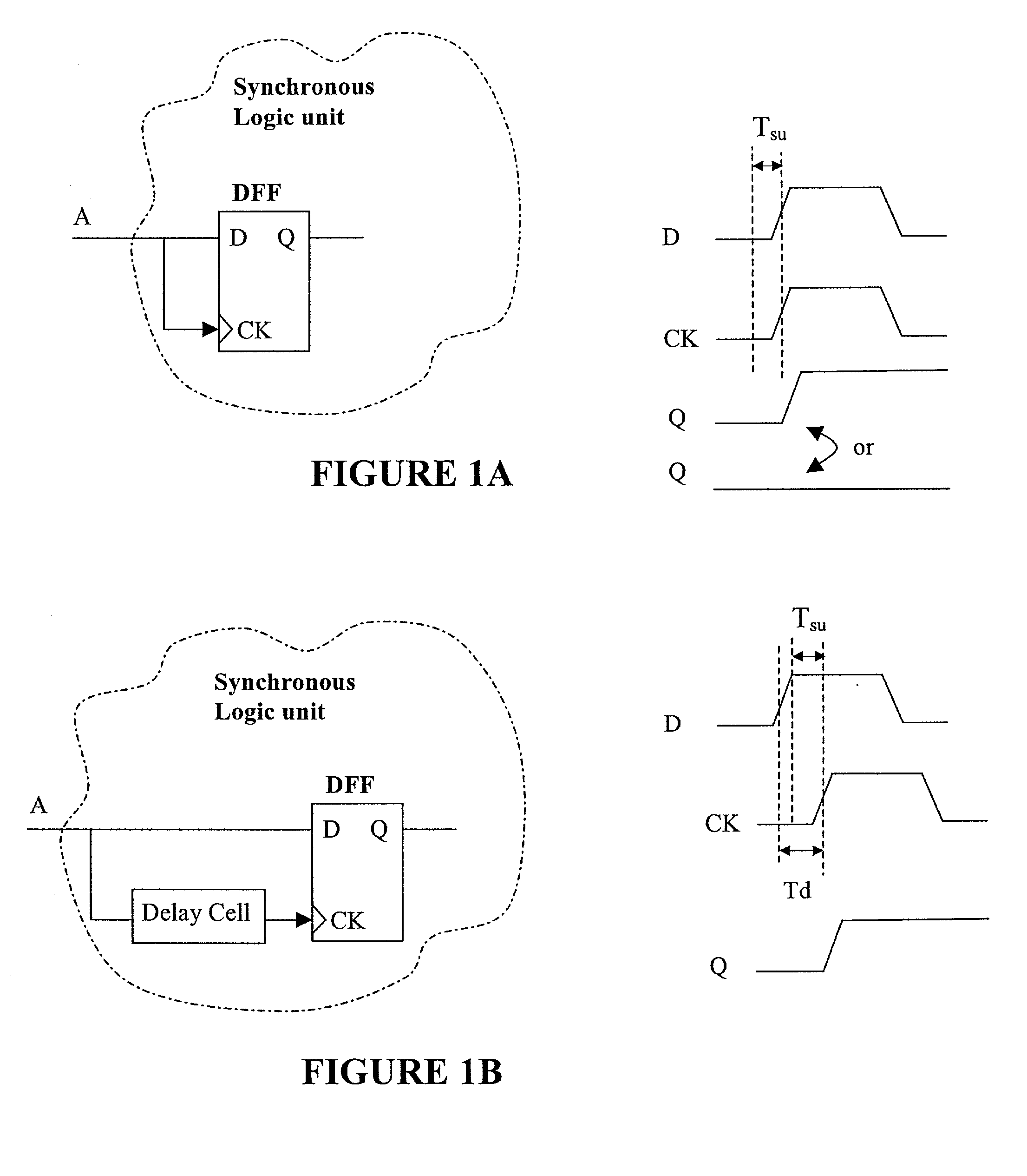
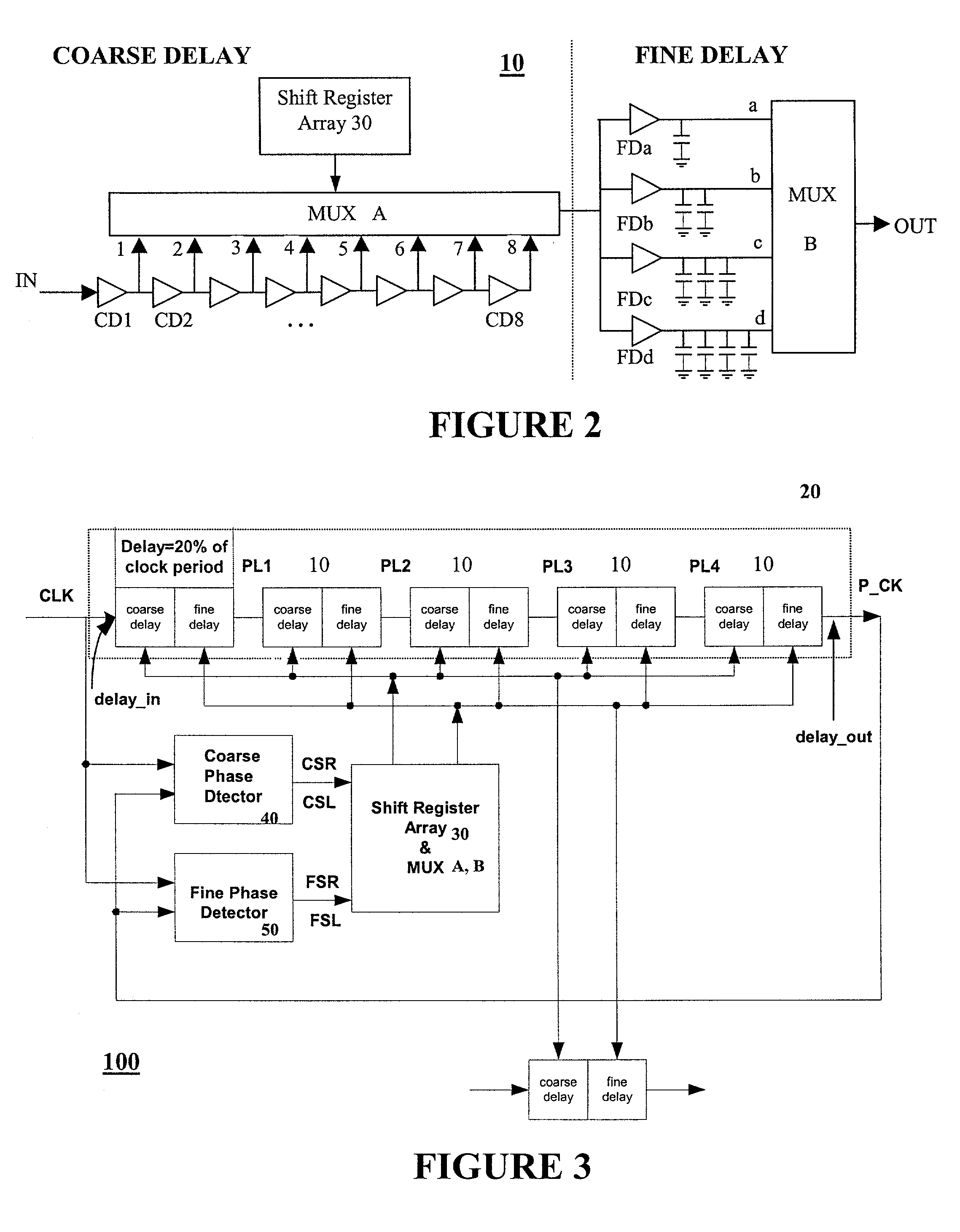
[0043] As described above, the present invention is directed to a delay compensation device, which measures the effects of PVT variations on a chip by measuring variations in the delay time of a delay component in the chip. The delay compensation circuit of the present invention can be utilized to program the delay time of the delay component and for providing information to be used in chip design to compensate for PVT conditions. Many of the figures referred to in connection with this detailed description contain similar components. The same reference labels will be used throughout the figures to denote similar components.

[0044] FIG. 5 illustrates a delay compensation circuit 60 according to an exemplary embodiment of the present invention. An input clock signal WCLK and reset signal RSTN are input to a single pulse generator 62. The input clock signal WCLK and the output of single pulse generator 62 are input to a two-input AND gate A1. The output signal D of AND gate A1 is fed to...


PUM


Abstract

A delay compensation circuit that determines the effects of process, voltage, and temperature (PVT) conditions of a chip by amplifying the maximum delay time of a delay element within the chip. The delay compensation circuit determines into which one of several predefined time intervals the amplified delay time falls, where each predefined time interval is associated with different PVT conditions. The delay compensation circuit of the present invention can be used to generate control signals for a variable delay element. Also, the PVT information provided by the delay compensation circuit can be used to design components within a chip to compensate for variances in PVT conditions. The feedback loop structure of the delay compensation device reduces the required chip area and power consumption of the delay compensation circuit.

Description

[0001] The present invention relates generally to synchronous circuit design, and more particularly, to a variable delay control circuit for providing a variable delay time to a clock signal to compensate for variations in the process, voltage and temperature (PVT) conditions of an integrated circuit.DESCRIPTION OF THE RELATED ART[0002] In digital circuits, synchronous logic elements operate by accepting and locking into a data signal during a transition of a clock signal. Such logic elements include D flip-flops, latch circuits, linear feedback shift registers (LFSRs), and counters. In order for a synchronous logic element to lock into a data signal, the signal must remain stable for some time prior to the clock edge, i.e., during a setup time. Also, the data signal usually must remain stable for some time after the clock edge, i.e., during a hold time, to be locked in by the synchronous logic element. If the data signal is not stable for both the setup time and the hold time of a ...

Claims


Application Information

Patent Timeline
Patent Type & Authority Applications(United States)
IPC IPC(8): H03K5/00H03K5/13H03K5/133H03L7/081H03L7/087
CPCH03K2005/00104H03L7/0805H03K5/133H03L7/087H03L7/0818H03L7/0814H03L7/0816
Inventor CAO, XIANGUODUARDO, OBEDYE, BO
Owner LUCENT TECH INC
Why Eureka
Try Eureka