Driver circuit
- Summary
- Abstract
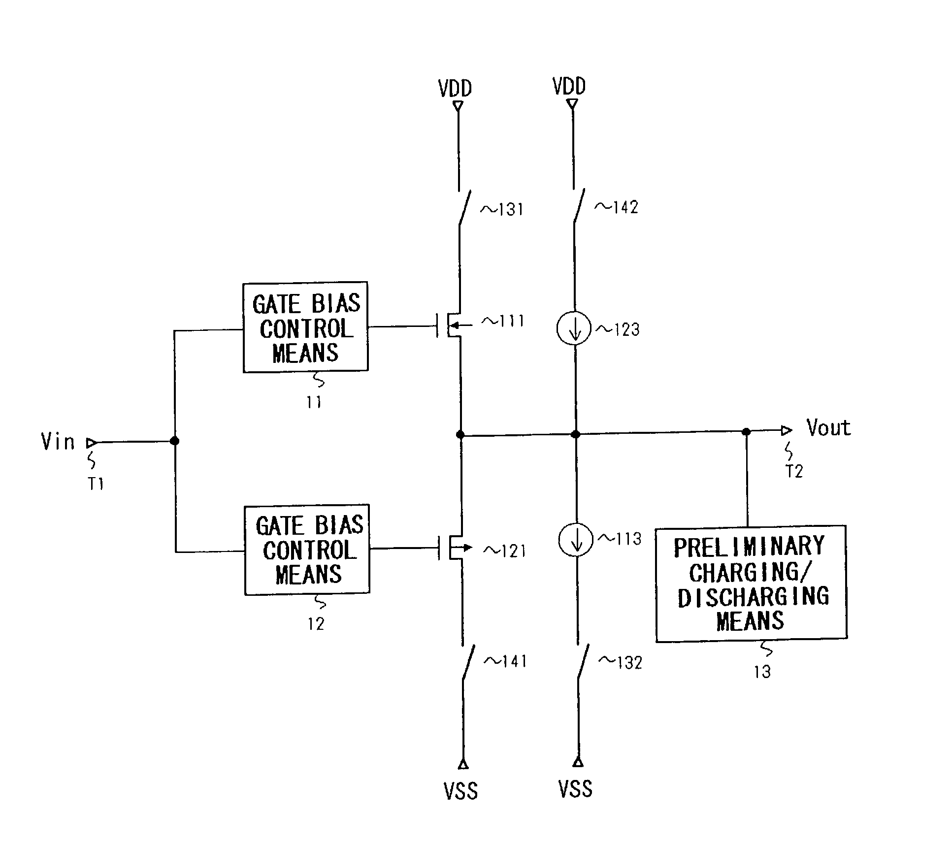
- Description
- Claims
- Application Information
AI Technical Summary
Benefits of technology
Problems solved by technology
Method used
Image

Examples
second embodiment
[0109] FIG. 6 is a diagram illustrating the structure of the present invention, in which components identical with those shown in FIG. 1 are designated by like reference characters.
[0110] As shown in FIG. 6, the driver circuit includes the N-channel MOS transistor 112 having its source connected to the input terminal T1 via the switch 133 and having its gate and drain tied together; the switch 134 and constant-current source 114 (P-channel MOS transistor) provided between the drain of the N-channel MOS transistor 112 and high-potential power supply VDD; and the N-channel MOS transistor 111 having a drain connected to the high-potential power supply VDD via the switch 131, a gate connected in common with the gate of the N-channel MOS transistor 112 and a source connected to the output terminal T2. The common gate of the N-channel MOS transistors 111, 112 is connected to the high-potential power supply VDD via the switch 136, the switch 145 and constant-current source 125 are connecte...
third embodiment
[0119] FIG. 7 is a diagram illustrating the structure of the present invention, in which components identical with those shown in FIG. 6 are designated by like reference characters. The driver circuit shown in FIG. 7 is obtained by eliminating the current sources 115 and 125 and the switches 135 and 145 from the driver circuit of FIG. 6 and adding on a P-channel MOS transistor 116 and an N-channel MOS transistor 126. The P-channel MOS transistor 116 has a source and drain connected to the gate (drain) and source, respectively, of the N-channel MOS transistor 112, and a gate to which the voltage BIASP is applied. The N-channel MOS transistor 126 has a source and drain connected to the gate (drain) and source, respectively, of the P-channel MOS transistor 122, and a gate to which the voltage BIASN is applied. The voltage BIASP is supplied also to the gates of the P-channel MOS transistors 114, 123 that constitute the constant-current sources. The voltage BIASN is supplied also to the ...
PUM
 Abstract
Description
Claims
Application Information
 - Generate Ideas
- Intellectual Property
- Life Sciences
- Materials
- Tech Scout
- Unparalleled Data Quality
- Higher Quality Content
- 60% Fewer Hallucinations
Browse by: Latest US Patents, China's latest patents, Technical Efficacy Thesaurus, Application Domain, Technology Topic, Popular Technical Reports.
© 2025 PatSnap. All rights reserved.Legal|Privacy policy|Modern Slavery Act Transparency Statement|Sitemap|About US| Contact US: help@patsnap.com