Oblique deposition apparatus

a deposition apparatus and oblique technology, applied in the direction of electrodes, chemical vapor deposition coatings, ion implantation coatings, etc., can solve the problems of unsatisfactory material passing through the opening, the difficulty of sputtering and the inability to achieve a deep conformal coverage within high aspect ratio steps or contacts

Inactive Publication Date: 2003-01-30
DATA STORAGE INST
View PDF0 Cites 35 Cited by
  • Summary
  • Abstract
  • Description
  • Claims
  • Application Information

AI Technical Summary

Problems solved by technology

As a result, it is difficult for sputtering to achieve a deep conformal coverage within high aspect ratio steps or contacts on semiconductor wafer substrate.
However, the collimator, like everything else within a sputtering chamber, gets coated with the sputtering material.
Eventually the amount of material able to pass through the openings may become unsatisfactory.
Existing techniques involving a collimator are effective in making the incident flux perpendicular to the substrate surface, but no such technique is available to make the incident flux oblique to the substrate surface (i e. an oblique sputtering deposition).
More so, there is no existing device for preparing thin films on a whole disk substrate to produce columns of film material angled in the circumferential direction or radial direction by using oblique sputtering deposition.

Method used


Image

  • Oblique deposition apparatus
  • Oblique deposition apparatus
  • Oblique deposition apparatus

Examples


first embodiment

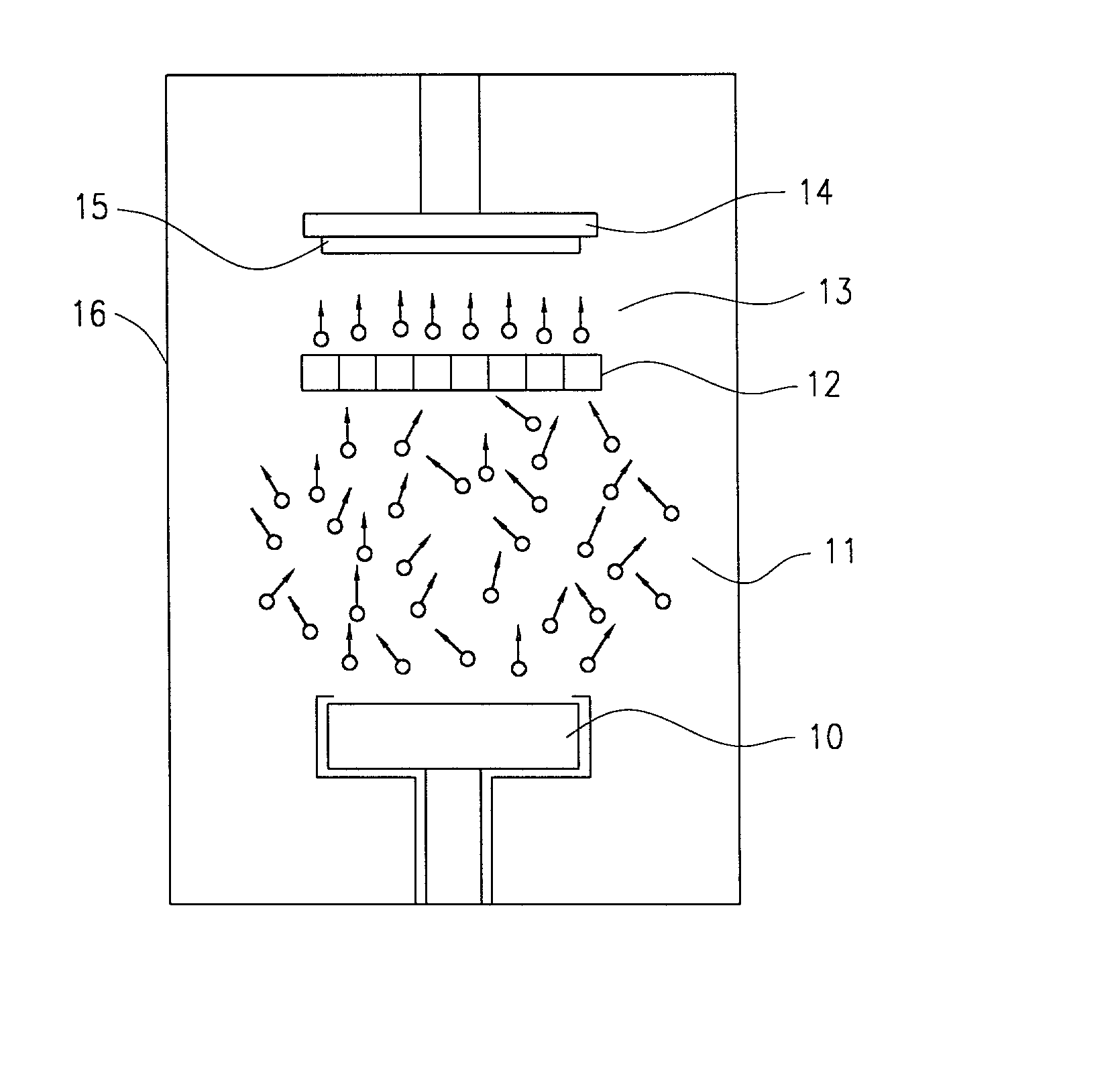
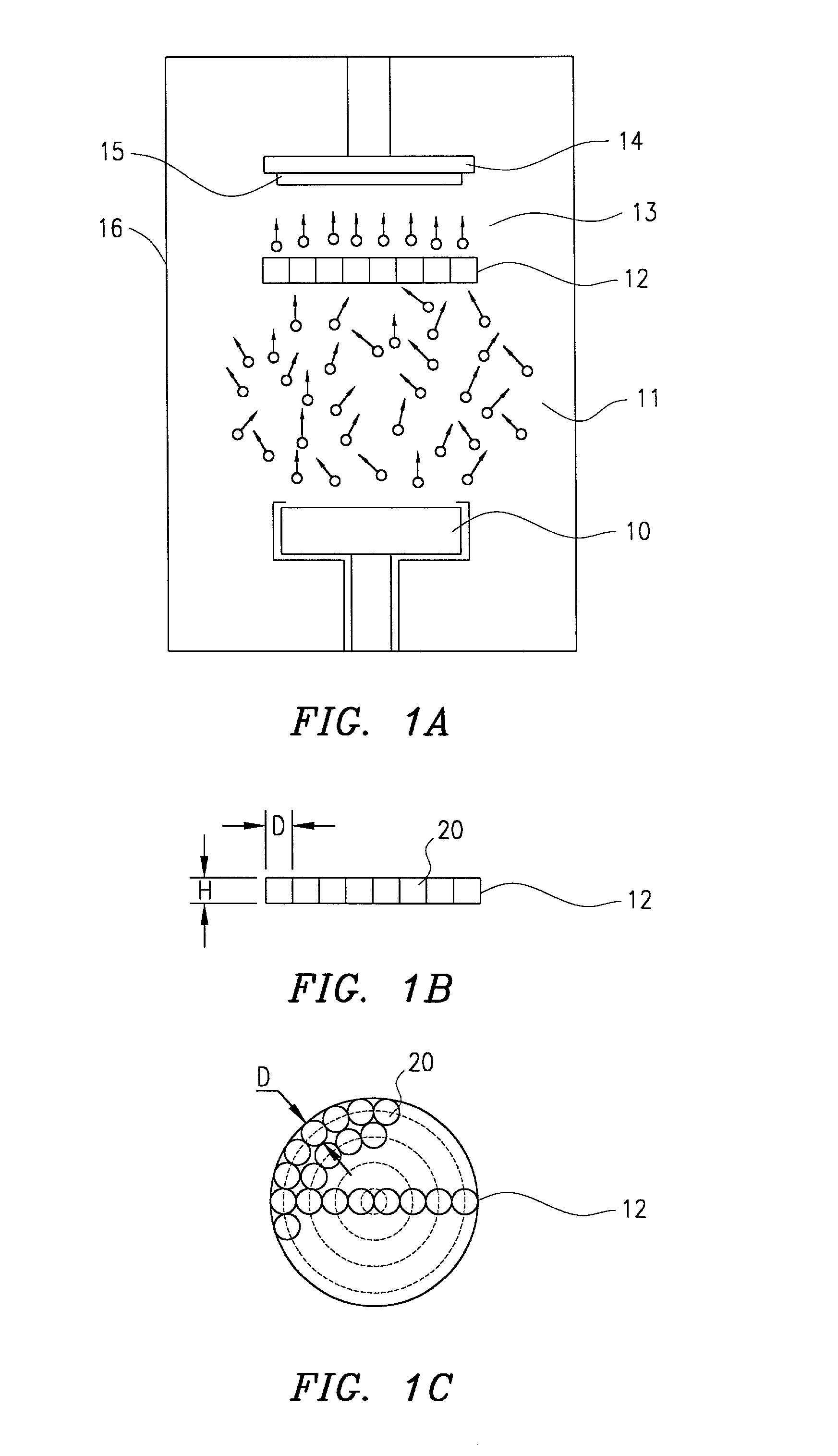
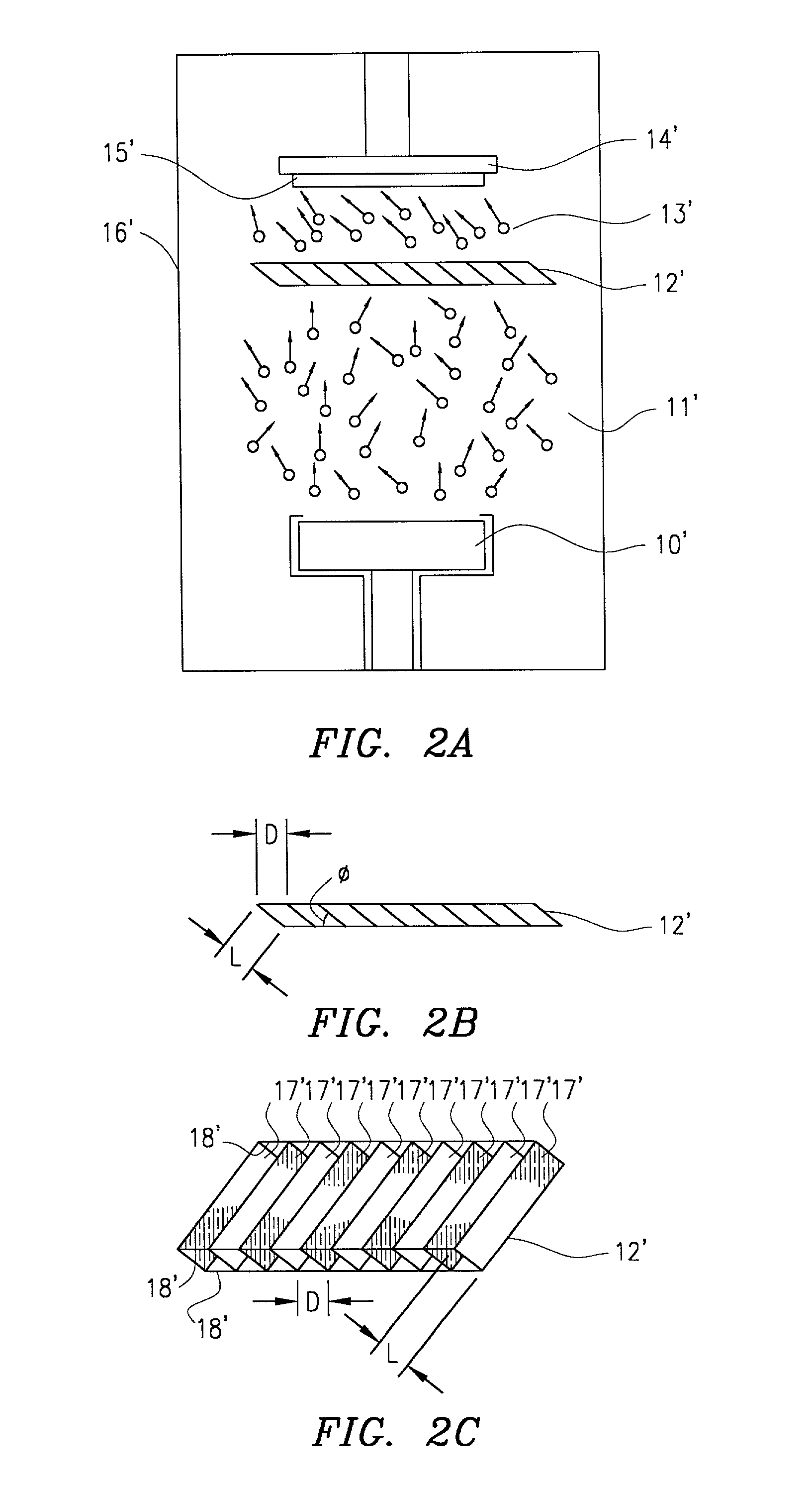
[0023] A cross-sectional view of the device in accordance with the present invention is illustrated in FIG. 2A. The difference between FIG. 1A and FIG. 2A is that in FIG. 2A an oblique collimator 12', rather than a perpendicular collimator, is shown. FIG. 2C is a 3-dimensional drawing of the collimator 12', which consists of supports 18' which span a plurality of rectangular sheets 17'. The collimator 12' can be constructed of metal or other conductor materials, insulate materials, or semiconductor materials. The number of the sheets 17' can be varied to achieve the desired passage size.

[0024] FIG. 2B is an end view of the collimator 12'. The collimator can be described by its aspect ratio D / L, and obliquing angle .theta., where D is the distance between two neighboring sheets 17', L is the width of a sheet 17' (i.e. the depth of the collimator), and .theta. the angle between the sheet 17' and the support 18'. As shown in FIG. 2A, the angled collimator 12' is placed between the subs...

second embodiment

[0025] the oblique collimator is illustrated in FIG. 3A. The collimator is made of a circular-shaped support 18" and a plurality of trapezoid-shaped sheets 17". Sheets 17" can be made of conductor, insulator or semiconductor materials. This circular-shaped collimator is specially designed for a disk-shaped substrate. The sheets 17" are angled in the circumferential direction.

[0026] FIG. 3B is a sheet 17" having an increasing width toward its outer end which corresponds with the outer diameter of the collimator. This design ensures that the aspect ratio of the collimator is the same everywhere, and results in a desirable uniformity of thickness and uniform oblique effect.

[0027] When this collimator is placed between a substrate and a target in a sputtering system similar to FIG. 2A, the resultant thin film on a disk substrate will have an angled column structure, as shown in FIG. 4. The columns angle in a circumferential direction with respect to the substrate surface of the disk sub...


PUM

PropertyMeasurementUnit
angleaaaaaaaaaa
oblique angleaaaaaaaaaa
heightaaaaaaaaaa

Abstract

An oblique sputtering deposition apparatus is provided for preparing a thin film. A collimator having angled passages for filtering out particles from stray directions is placed between the substrate and the incident particle flux. The angle of the passages can be adjusted from about 0 to about 90° with respect to the substrate normal according to requirements. The oblique incidence of particle flux brings forms a column structure which is also angled.

Description

[0001] 1. Field of the Invention[0002] The present invention relates to depositing films, and more particularly to an apparatus for preparing thin films by an oblique collimator deposition.[0003] 2. Description of the Prior Art[0004] Sputtering is a commonly used method for thin film deposition. Sputtering is performed by providing ionized atoms, such as Ar.sup.+, in a vacuum which accelerate towards and bombard a negatively-charged target material. The ionized atoms knock off other atoms and molecules from the target material. These ejected atoms and molecules subsequently deposit on a pre-selected substrate also disposed in the vacuum chamber, thus forming a film on a surface of the substrate.[0005] The trajectory of the ejected atoms and molecules depends in significant part on the incident angle of the bombarding ions and the scattering of ejected atoms and molecules as they collide with other particles. The trajectory follows a well-known cosine (or Gaussian) distribution. Ther...

Claims


Application Information

Patent Timeline
Patent Type & Authority Applications(United States)
IPC IPC(8): C23C14/22C23C14/34H01J37/34
CPCC23C14/225C23C14/34H01J37/34H01J37/3447
Inventor WANG, JIAN-PINGSHI, JIANZHONG
Owner DATA STORAGE INST
Why Eureka
Try Eureka