Semiconductor device and method of fabricating the same

a technology of semiconductors and semiconductors, applied in the direction of semiconductor devices, electrical equipment, transistors, etc., can solve the problems of low concentration of dopant, deterioration of current driving capability in n-channel mosfet, and decrement of electron mobility

Inactive Publication Date: 2003-02-27
NEC ELECTRONICS CORP
View PDF0 Cites 878 Cited by
  • Summary
  • Abstract
  • Description
  • Claims
  • Application Information

AI Technical Summary

Problems solved by technology

Thus, a problem that the electron mobility degrades occurs.
Due to this reason, the saturation drain current I.sub.dsat decreases and as a result, the current driving capability deteriorates in the n-channel MOSFET.
However, the concentration of the dopant is very small.
Since the first nitride layer having an actual or genuine tensile stress is not formed on the whole surface of the substrate, the possibility that the first nitride layer is detached from the substrate and damaged is significantly decreased.

Method used


Image

  • Semiconductor device and method of fabricating the same
  • Semiconductor device and method of fabricating the same
  • Semiconductor device and method of fabricating the same

Examples


first embodiment

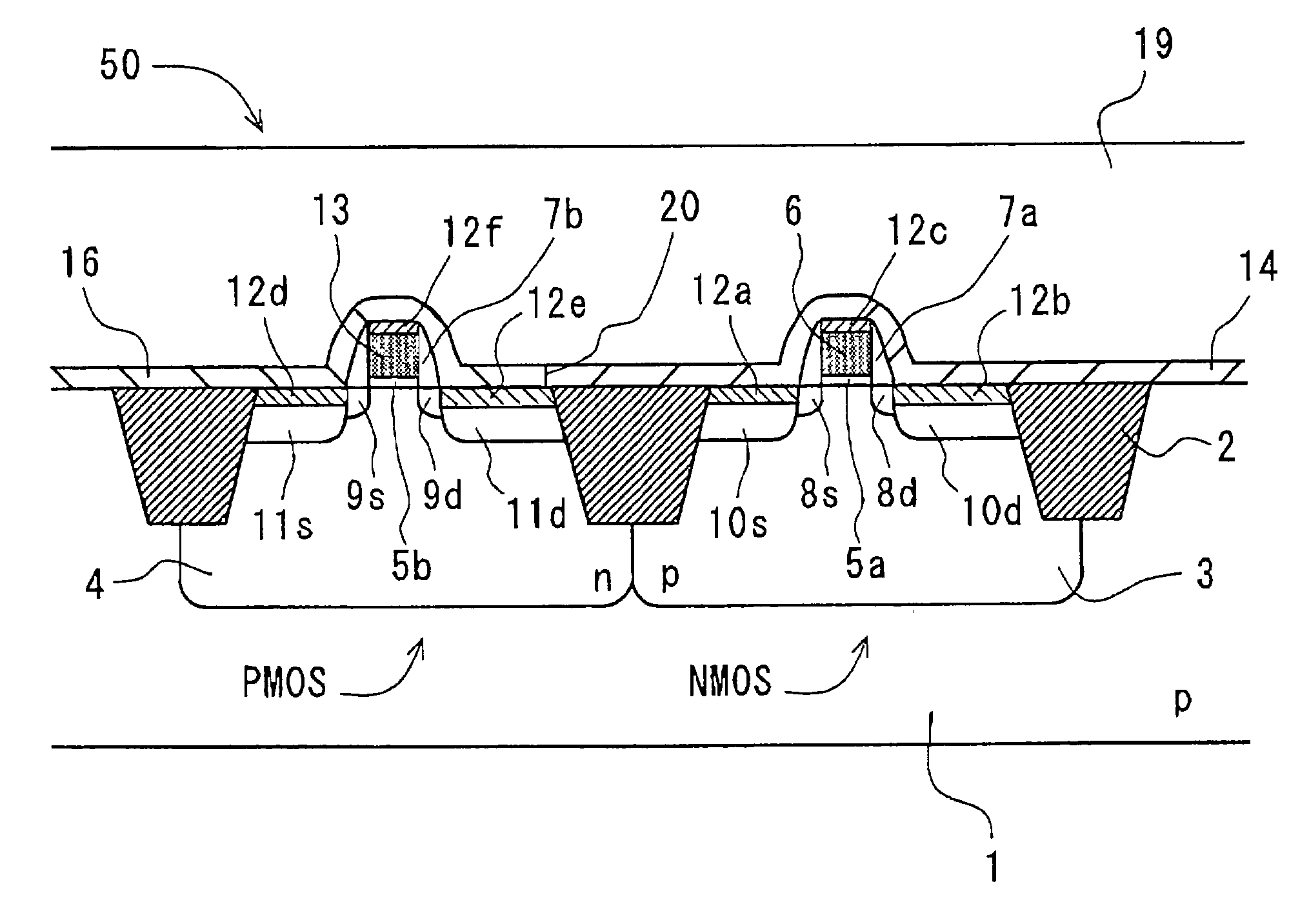
[0083] FIG. 2 shows the structure of a semiconductor device 50 having a n-channel MOSFET and a p-channel MOSFET according to a first embodiment of the invention. Actually, the device 50 comprises other n-channel MOSFETs and other p-channel MOSFETs on the same semiconductor substrate. However, one of the n-channel MOSFETs and one of the p-channel MOSFETs are shown and explained below for the sake of simplification.

[0084] As shown in FIG. 2, the semiconductor device 50 comprises a p-type single-crystal Si substrate 1 on which a n-channel MOSFET and a p-channel MOSFET are formed.

[0085] An isolation region 2 is selectively formed in a recess or recesses of the substrate 1, thereby forming an active region in which the n-channel MOSFET (i.e., NMOS) is formed and an active region in which the p-channel MOSFET (i.e., PMOS) is formed. In the active region for the n-channel MOSFET, a p-type well 3 is formed. In the active region for the p-channel MOSFET, a n-type well 4 is formed.

[0086] In t...

second embodiment

[0112] FIG. 5 shows the structure of a semiconductor device 50A having a n-channel MOSFET and a p-channel MOSFET according to a second embodiment of the invention. This device 50A has the same structure as the device 50 of the first embodiment except that the SiN.sub.x layer 16 having an actual compressive stress is formed to cover the whole surface of the substrate 1. Therefore, the explanation on the same structure is omitted here for the sake of simplification by attaching the same reference symbols as those used in the first embodiment.

[0113] As seen from FIG. 5, the SiN.sub.x layer 16 is placed on the SiN.sub.x layer 14 in the area just above the n-channel-MOSFET. In other words, the layer 16 is overlapped with the underlying layer 14.

[0114] A method of fabricating the semiconductor device 50A according to the second embodiment of FIG. 5 is explained below.

[0115] First, as shown in FIG. 3A, the n- and p-channel MOSFETs are formed through the same process steps as those in the p...


PUM

PropertyMeasurementUnit
tensile stressaaaaaaaaaa
compressive stressaaaaaaaaaa
surface areaaaaaaaaaaa

Abstract

A semiconductor device improves the electron mobility in the n-channel MOSFET and reduces the bend or warp of the semiconductor substrate or wafer. The fist nitride layer having a tensile stress is formed on the substrate to cover the n-channel MOSFET. The tensile stress of the first nitride layer serves to relax a compressive stress existing in the channel region. The second nitride layer having an actual compressive stress is formed on the substrate to cover the p-channel MOSFET. The first and second nitride layers serve to decrease bend or warp of the substrate. Preferably, the first nitride layer is a nitride layer of Si formed by a LPCVD process, and the second nitride layer is a nitride layer of Si formed by a PECVD process.

Description

[0001] 1. Field of the Invention[0002] The present invention relates generally to semiconductor devices. More particularly, the invention relates to a semiconductor device having a n-channel Metal-Oxide-Semiconductor Field-Effect Transistor (MOSFET) and a p-channel MOSFET on a silicon (Si) substrate, and a method of fabricating the device.[0003] 2. Description of the Related Art[0004] FIGS. 1A to 1E show the process steps of a method of fabricating a known semiconductor device having a n-channel MOSFET and a p-channel MOSFET on a single-crystal Si substrate.[0005] First, as shown in FIG. 1A, a desired recess or recesses are formed in the surface area of a p-type single-crystal Si substrate 101 using a patterned silicon nitride (SiN.sub.x) layer (not shown) as a mask by a Reactive Ion Etching (RIE) process. Then, a silicon dioxide (SiO.sub.2) layer (not shown) is grown on the surface of the substrate 101 by using a High-Density Plasma source. The surface of the substrate 101 on which...

Claims


Application Information

Patent Timeline
Patent Type & Authority Applications(United States)
IPC IPC(8): H01L29/78H01L21/318H01L21/8238H01L27/092
CPCH01L21/823807H01L29/665H01L29/7843
Inventor SAITOH, TAKEHIRO
Owner NEC ELECTRONICS CORP
Why Eureka
Try Eureka