Electronic device and method for manufacturing the same, and method for shielding printed circuit board
a printed circuit board and electronic device technology, applied in the direction of flexible screening containers, coupling device connections, electrical apparatus construction details, etc., can solve the problems of not being widely used in general in respect of cost or availability, generating a big noise, and not being able to achieve the effect of suppressing the high frequency noise generated in the ground plane of the printed circuit board
- Summary
- Abstract
- Description
- Claims
- Application Information
AI Technical Summary
Benefits of technology
Problems solved by technology
Method used
Image
Examples
first embodiment
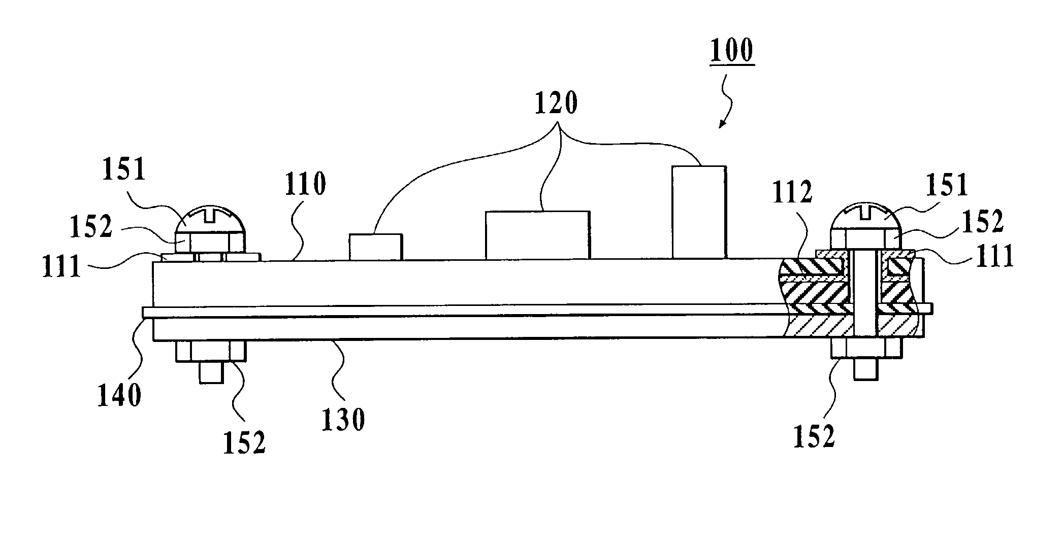
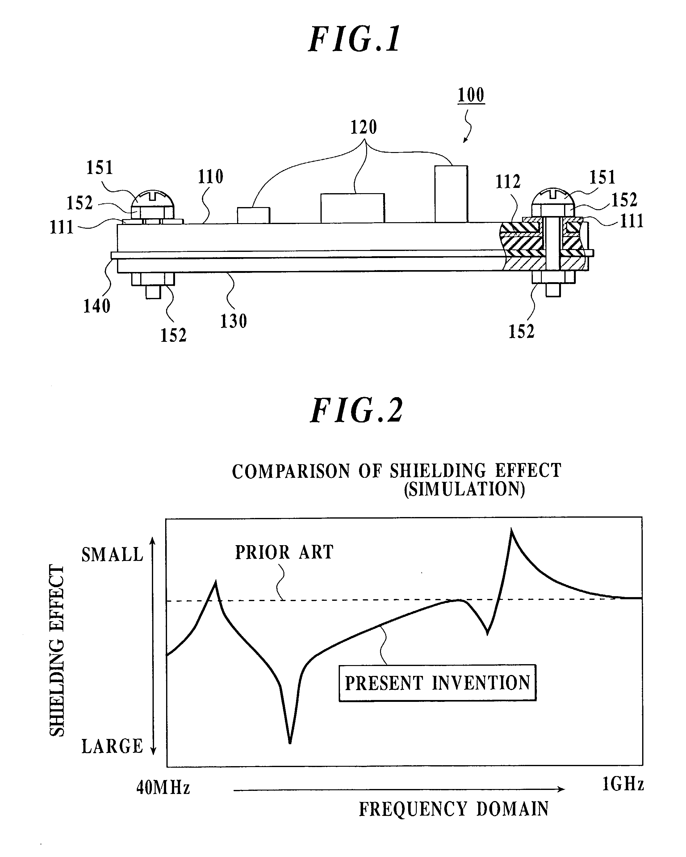
[0038] Hereinafter, the present invention will be explained with reference to FIG. 1.
[0039] In an electronic device 100 of the embodiment, as shown in FIG. 1, a shielding plate (electromagnetic shielding layer) 130 is adhered to a printed circuit board 110 through a thin insulating sheet (electrically insulating layer) 140. Moreover, in order to conduct electrically a ground pattern (ground) 111 of the printed circuit board 110 to the shielding plate 130 certainly, a resist in a portion of the ground pattern 111 is completely removed. The ground pattern 111 and the shielding plate 130 are tightened with bolts 151 and nuts 152, which are metal screws, so that they are electrically conducted completely. Therefore, the shielding plate 130 functions as a return path of signals which flow the wiring patterns (not shown) of the printed circuit board 110. Thereby, the same effect as increasing one layer of a ground layer of the printed circuit board 110 can be obtained. In addition, the re...
second embodiment
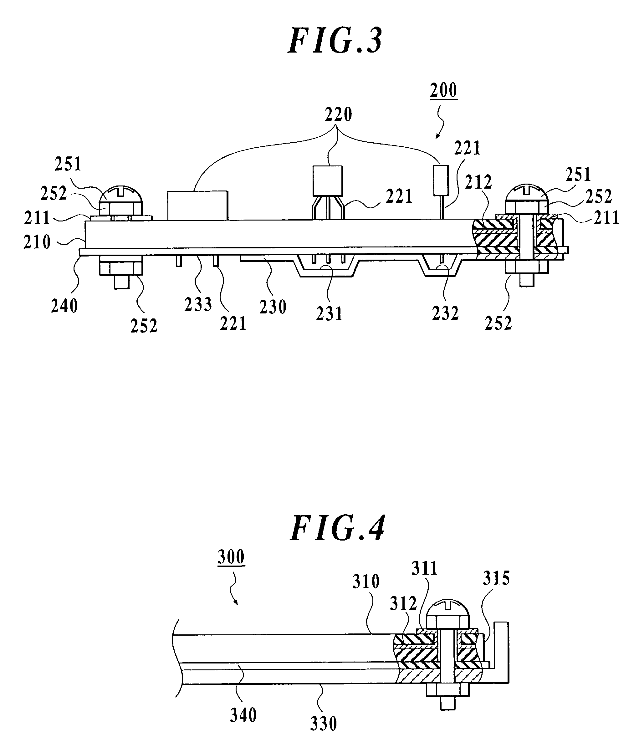
[0045] Next, the present invention will be explained with reference to FIG. 3.
[0046] In an electronic device 200 of the embodiment, as shown in FIG. 3, a shielding plate 230 provided with hollows 231 and 232 and a hole 233 is adhered to a printed circuit board 210 through an insulating sheet 240. The reason for providing the hollows 231 and 232 and the hole 233 is because unlike the case shown in FIG. 1, leads 221 of mounted electronic parts 220 may pass through the printed circuit board 210 or the insulating sheet 240 and may hit a shielding plate, when inserting the mounted electronic parts 220 in the printed circuit board 210. Thereby, the leads 221 provided on the electronic parts 220 for being mounted on the printed circuit board 210 will not be broken by hitting the shielding plate 230 even though the leads 221 pass through the printed circuit board 210 or the insulating sheet 240. Further, in the embodiment, since a ground pattern 211 of the printed circuit board 210 and the ...
third embodiment
[0048] Next, the present invention will be explained with reference to FIG. 4.
[0049] In an electronic device 300 of the embodiment, as shown in FIG. 4, a shielding plate 330 adhered to a printed circuit board 310 through an insulating sheet 340 has a shape of covering an end face 315 of the printed circuit board 310. Further, in the embodiment, a ground pattern 311 of the printed circuit board 310 and the shielding plate 330 are also electrically conducted through bolts 351 and nuts 352, which are metal screws. Thereby, the same effect as the above-described first and second embodiments can be obtained. Moreover, the electromagnetic noise can be prevented from radiating from the end face 315 of the printed circuit board 310. In particular, it has a great effect in preventing the radiation of the electromagnetic noise in a multi-layer printed circuit board. In addition, the reference numeral 312 in FIG. 4 indicates a ground plane of the printed circuit board 310.
[0050] Further, in th...
PUM
 Abstract
Description
Claims
Application Information


