Wafer level interconnection

a technology of microelectromechanical systems and wafers, applied in the field of rf mems (microelectromechanical system) technology, can solve the problems of many hetero-junction technologies, epitaxial methods, and substrate materials that are considered incompatible with rf mems fabrication technology, and the rf performance of the circuit can be limited

Inactive Publication Date: 2003-03-13
RAYTHEON CO
View PDF0 Cites 100 Cited by
  • Summary
  • Abstract
  • Description
  • Claims
  • Application Information

AI Technical Summary

Problems solved by technology

Many hetero-junction technologies, epitaxial methods, and substrate materials have been considered incompatible.
Specifically, RF MEMS fabrication technology has been considered incompatible with silicon germanium (SiGe) fabrication technology.
The primary technical challenge associated with direct integration RF MEMS circuitry with sophisticated electronics is overcoming the influence of the low-resistivity substrate material, typically used by SiGe manufacturers, on the insertion loss of the RF MEMS circuit.
DI, however, has a number of technical challenges.
Secondly, the RF performance of the circuit can be limited by the thin microwave dielectric layer.

Method used


Image

  • Wafer level interconnection
  • Wafer level interconnection

Examples


Embodiment Construction

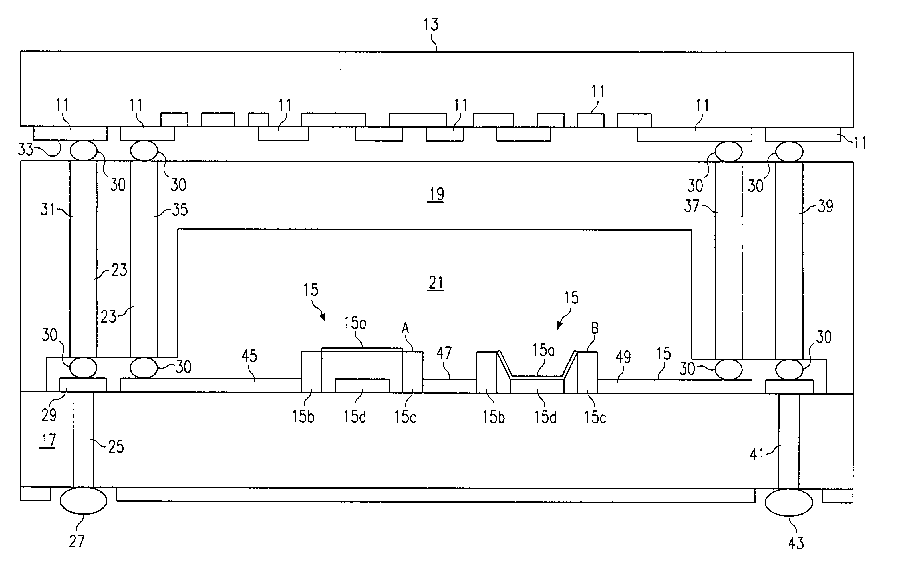
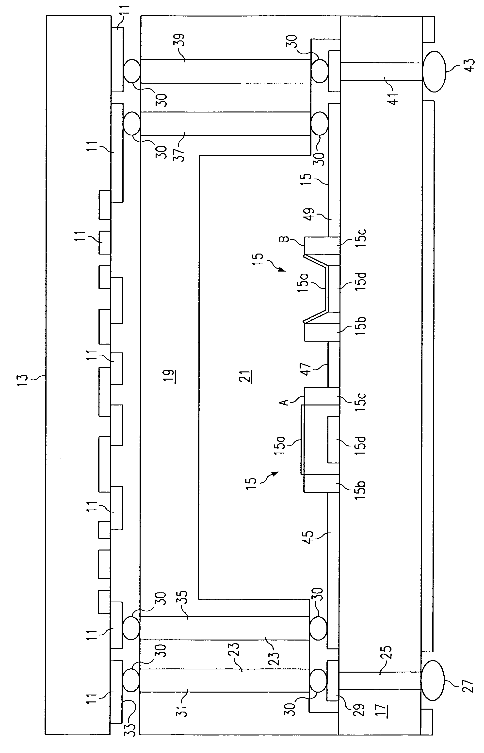
[0017] According to one embodiment of the present invention illustrated in FIG. 1 vertical electrical interconnection between the electronics circuitry 11 on one low-resistivity SiGe substrate 13 and RF MEMS circuitry 15 on a separate high resistivity silicon (HR) substrate 17. The low-resistivity substrate material 13 may also be silicon CMOS or gallium arsenide (GaAS) substrate. This is accomplished by using wafer fabrication techniques to construct a conductive metalization layer on either the primary (i.e., RF MEMS) substrate 17 or the secondary (i.e., other electronics) substrate 13. A dielectric lid 19 is spaced between the electronics circuitry 11 on the substrate 13 and the high resistivity substrate 17 and provides a canopy or lid over the RF MEMS circuitry 15 leaving a gap 21 over the RF MEMS circuitry 15. The gap 21 is filled with an inert environment such as a gas such as nitrogen or a vacuum. The lid 19 may be made of Pyrex, quartz or glass and is made of a material wit...


PUM


Abstract

RF MicroElectroMechanical Systems (MEMS) circuitry (15) on a first high resistivity substrate (17) is combined with circuitry (11) on a second low resistivity substrate (13) by overlapping the first high resistivity substrate (17) and MEMS circuitry (15) with the low resistivity substrate (13) and circuitry (11) with the MEMS circuitry (15) facing the second circuitry (11). A dielectric lid (19) is placed over the MEMS circuitry (15) and between the first substrate (17) and second substrate (13) with an inert gas in a gap (21) over the MEMS circuitry (15). Interconnecting conductors (25, 31, 35, 37, 39, 41) extend perpendicular and through the high resistivity substrate (17) and through the dielectric lid (19) to make electrical connection with the low resistivity substrate (13).

Description

[0001] This application is a continuation of U.S. Ser. No. 09 / 756,801 filed Jan. 10, 2001 entitled WAFER LEVEL INTERCONNECTION, now U.S. Pat. No. ______.[0002] 1. Field of the Invention[0003] This invention relates to RF MEMS (MicroElectroMechanical Systems) technology and more particularly to MEMS with wafer level interconnection to electronics on low-resistivity substrate material.[0004] 2. Background of Invention[0005] RF MEMS technology has been targeted for insertion in a wide range of military applications from multi-band multi-mode communication systems to inertial navigation systems to sensors. In fact, RF MEMS technology insertion plays a major role in numerous current DARPA funded programs such as Ultra Comm and the Airborne Communications Node (ACN).[0006] This technology could be applied to these programs plus new military insertion opportunities such as targeting systems, satellite communications, high speed tactical data link systems, electronic warfare and countermeas...

Claims


Application Information

Patent Timeline
Patent Type & Authority Applications(United States)
IPC IPC(8): B81B7/00B81B7/02H01H59/00H01L23/04H01L25/065H05K1/03H05K1/14
CPCB81B7/0006H01L23/04H01L25/0657H01L2225/06517H01L2225/0652H01L2225/06572H01L2225/06586H01L2924/0002H01L2924/00H01L23/52
Inventor CHEEVER, JAMES L.GOLDSMITH, CHARLES L.EHMKE, JOHN C.ABLES, BILLY D.
Owner RAYTHEON CO
Why Eureka
Try Eureka