

Ultra-high speed, active polymer-silica hybrid, single control voltage MMI-based 1-by-N packet switch and WG-based WDM packet router/TDM converter and methods of making same
a polymer and active technology, applied in the field of fiber optic devices, can solve the problems of low speed, low loss, and passive material with no electrically controlled phase shifting ability
- Summary
- Abstract
- Description
- Claims
- Application Information
AI Technical Summary
Problems solved by technology
Method used
Image

Examples
Embodiment Construction
[0017] Illustrative embodiments and exemplary applications will now be described with reference to the accompanying drawings to disclose the advantageous teachings of the present invention.
[0018] While the present invention is described herein with reference to illustrative embodiments for particular applications, it should be understood that the invention is not limited thereto. Those having ordinary skill in the art and access to the teachings provided herein will recognize additional modifications, applications, and embodiments within the scope thereof and additional fields in which the present invention would be of significant utility.
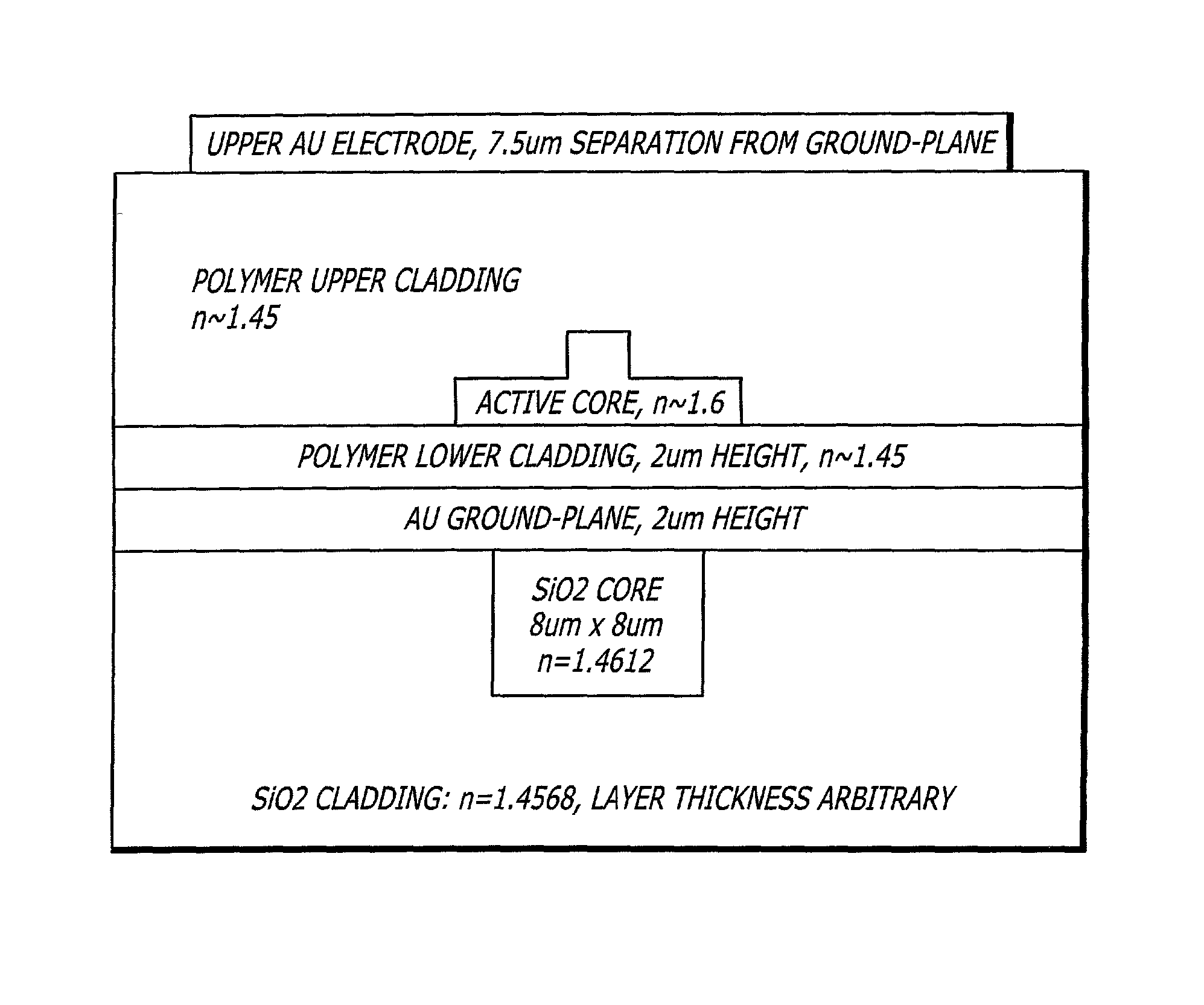
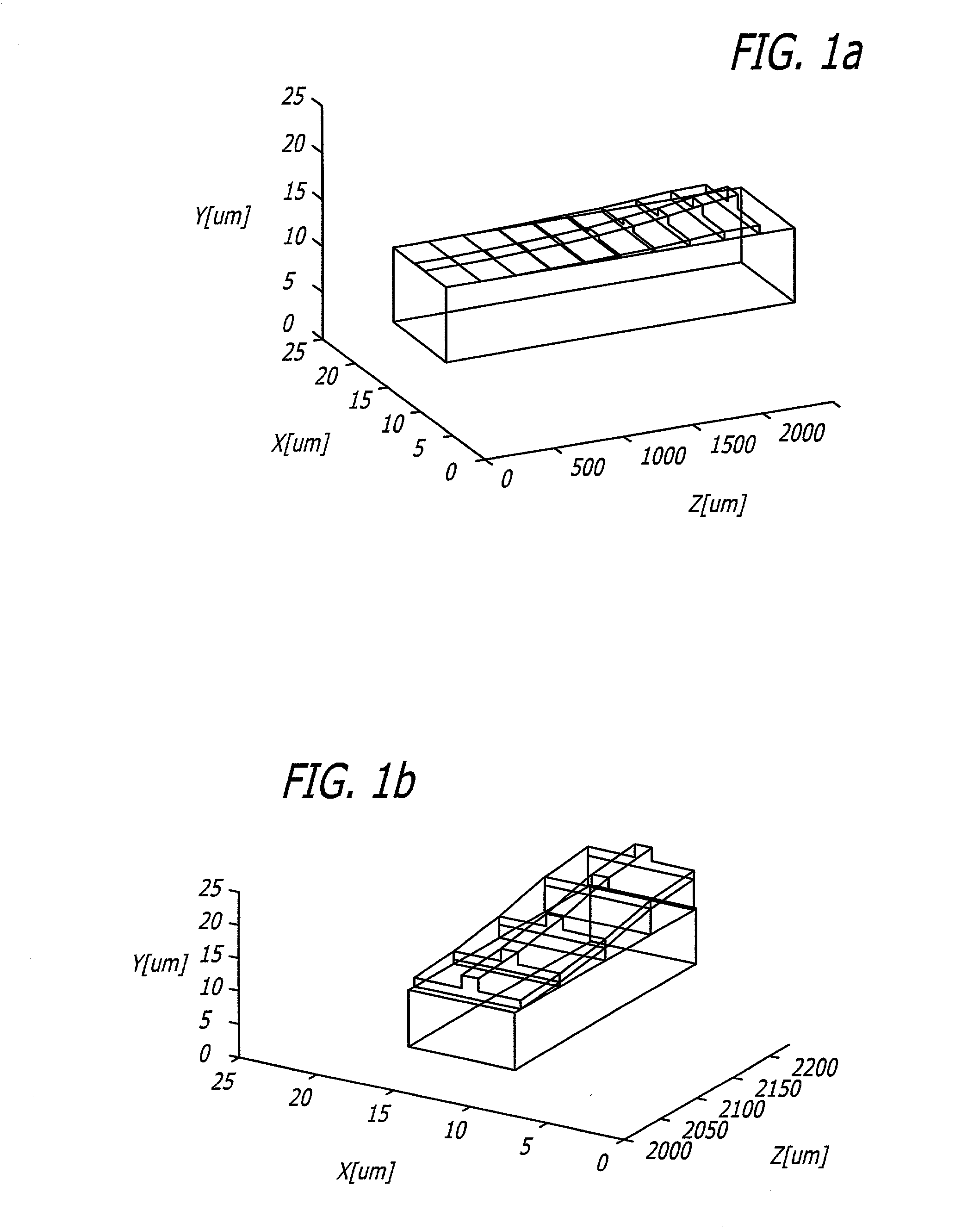
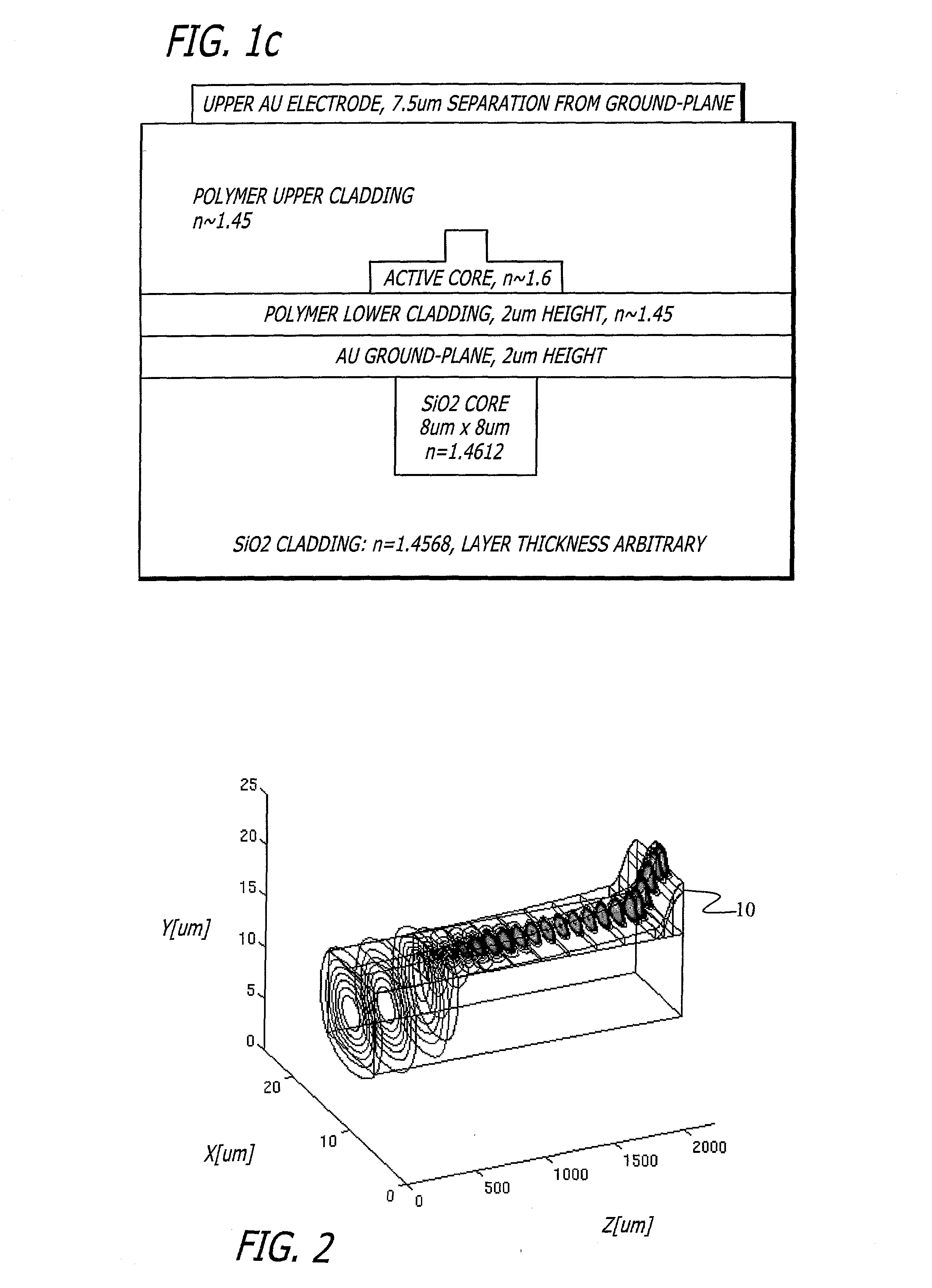
[0019] The present invention addresses the above-identified need in the art by providing a hybrid solution, with low loss silica routing signals to and from active sections which can provide wideband index modulation. Two leading conventional modulation mechanisms for telecommunication wavelengths, LiNbO3 and InP, are both poorly suited for hybrid ...
PUM
| Property | Measurement | Unit |
|---|---|---|
| thickness | aaaaa | aaaaa |
| thickness | aaaaa | aaaaa |
| microstrip impedance | aaaaa | aaaaa |
Abstract
Description
Claims
Application Information