Body contact mosfet

a contact transistor and body technology, applied in the field of field effect transistors, can solve the problems of hysteresis, poor performance, decreased performance,

Inactive Publication Date: 2003-07-31
GLOBALFOUNDRIES US INC
View PDF1 Cites 73 Cited by
  • Summary
  • Abstract
  • Description
  • Claims
  • Application Information

AI Technical Summary

Problems solved by technology

SOI technology where the body is not connected to anything-called a floating body device-may suffer from the problem of hysteresis: the body retains charge and some of the electrical properties from the last time the transistor was used, interfering with subsequent use of the device.
This approach leads to decreased performance in that it yields a greatly increased gate capacitance over a conventional device, often leading to very poor performance.

Method used


Image

  • Body contact mosfet
  • Body contact mosfet
  • Body contact mosfet

Examples


Embodiment Construction

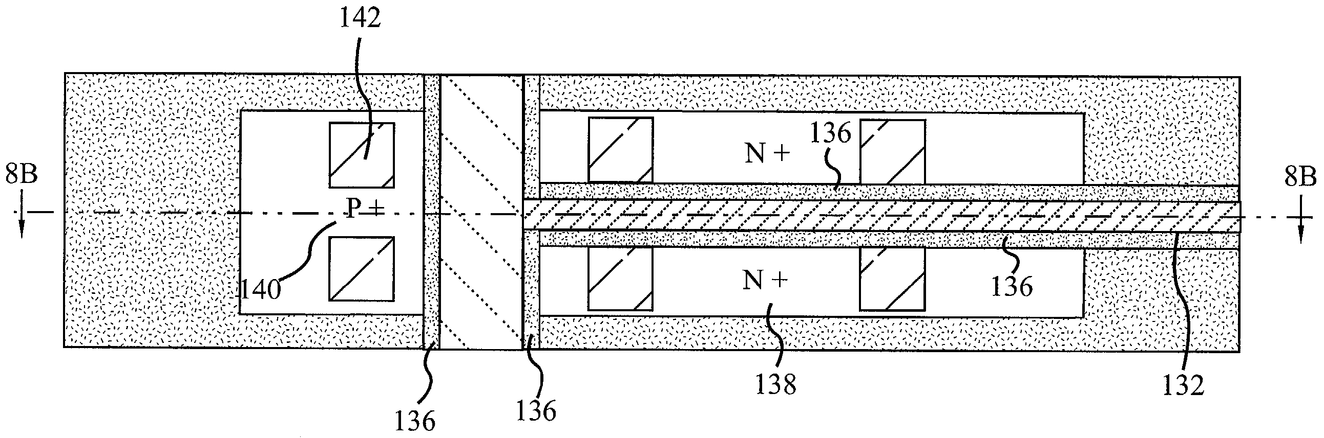
[0024] As has been previously stated, the present invention provides a body contact structure that overcomes the disadvantages of the prior art. The present invention utilizes an insulator structure between the body contact portion of the active area and the transistor portion. In particular, the present invention provides a raised insulative structure, comprising an element distinct from the gate, formed across the active area that isolates the portion of the area where transistors are formed from the portions of the active area where the body contact is formed. The body contact thus produced adds no significant gate capacitance to the gate. The transistor and body contact portions are formed in a substantially coplanar semiconducting substrate.

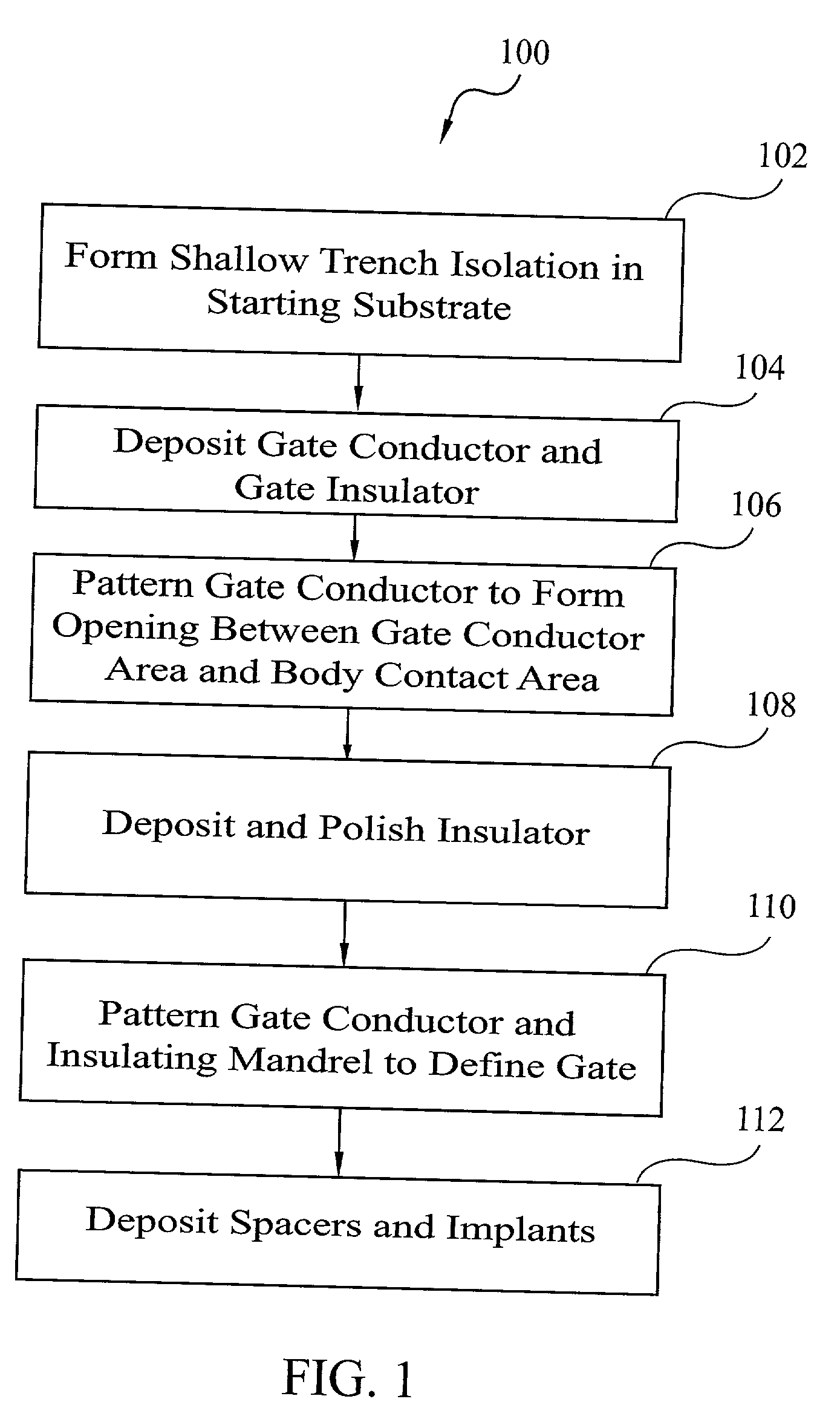
[0025] The present invention can be implemented using a variety of fabrication methods. These methods form the insulative structure between the transistor portion of the active area and the body contact portion of the active area in a variet...


PUM


Abstract

A body contact structure utilizing an insulating structure between the body contact portion of the active area and the transistor portion of the active area is disclosed. In one embodiment, the present invention substitutes an insulator for at least a portion of the gate layer in the regions between the transistor and the body contact. In another embodiment, a portion of the gate layer is removed and replaced with an insulative layer in regions between the transistor and the body contact. In still another embodiment, the insulative structure is formed by forming multiple layers of gate dielectric between the gate and the body in regions between the transistor and the body contact. The body contact produced by these methods adds no significant gate capacitance to the gate.

Description

[0001] 1. Technical Field[0002] This invention generally relates to field effect transistors, and more specifically relates to body contact field effect transistors formed in silicon-on-insulator technology.[0003] 2. Background Art[0004] A conventional transistor has a source region and a drain region spaced apart by an intervening body region. All of these regions are planar, and are controlled by a gate. The body region is the area from which electron hole pair generation takes place that allows current to be carried between the source and drain regions underneath the gate. By contacting the body region, a charge may be applied that changes the voltage at which the transistor turns on. This is often referred to as a Vt adjustment because the threshold voltage of the device is being adjusted with this technique.[0005] Silicon-on-insulator (SOI) technology employs a layer of semiconductor material overlying an insulation layer on a supporting bulk wafer. Typically, the structure com...

Claims


Application Information

Patent Timeline
Patent Type & Authority Applications(United States)
IPC IPC(8): H01L21/336H01L29/786
CPCH01L29/78615H01L29/66772
Inventor BRYANT, ANDRESCOTTRELL, PETER E.ELLIS-MONAGHAN, JOHN J.GAUTHIER, ROBERT J. JR.NOWAK, EDWARD J.RANKIN, JED H.ASSADERAGHI, FARIBORZ
Owner GLOBALFOUNDRIES US INC
Why Eureka
Try Eureka