Global planarization method
- Summary
- Abstract
- Description
- Claims
- Application Information
AI Technical Summary
Problems solved by technology
Method used
Image

Examples
Embodiment Construction
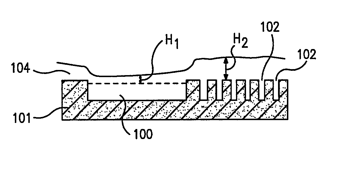
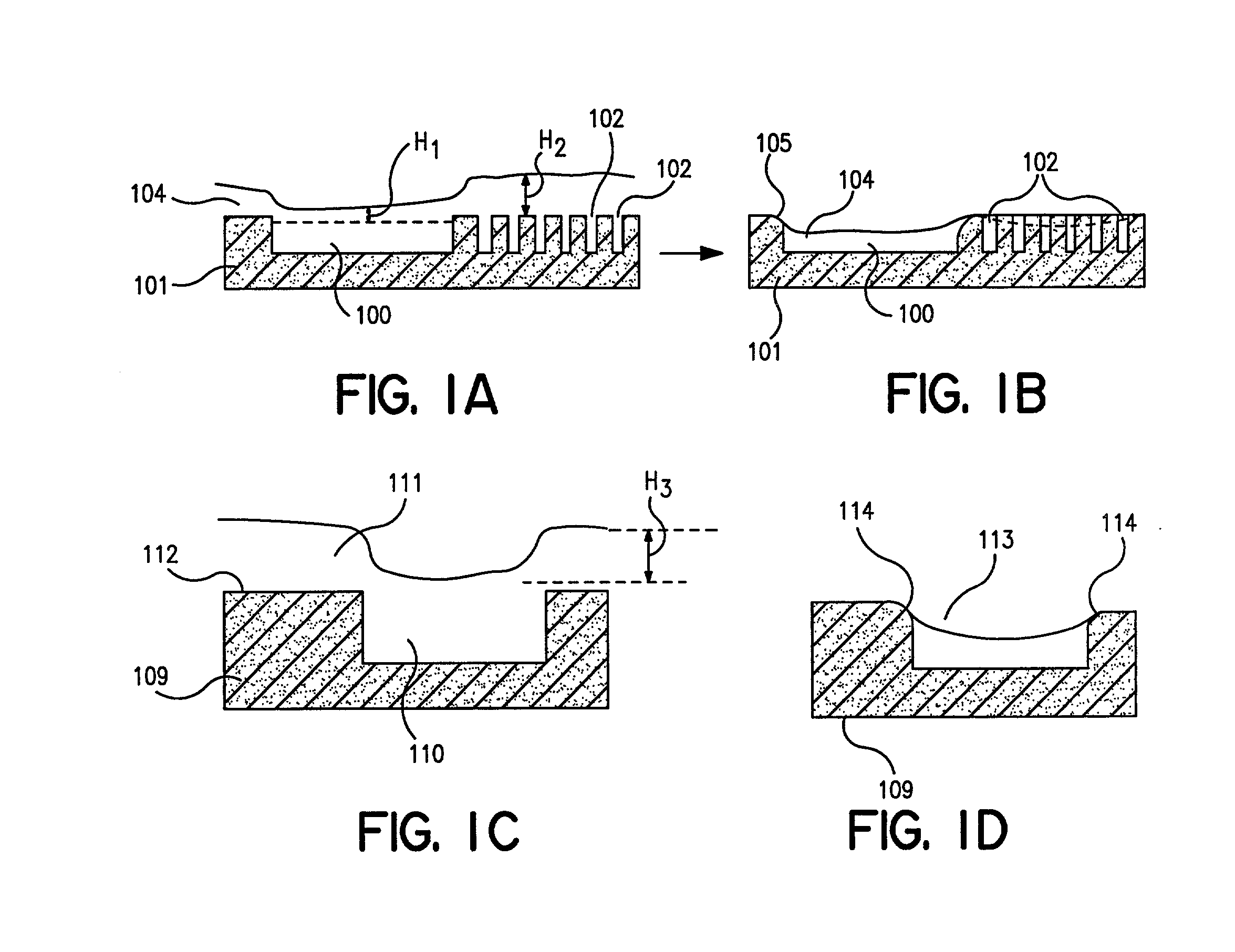
[0014] The present invention concerns methods for manufacturing substrates having features that create planarization difficulties. Such features include large step-height features, large width features, a low density of features in proximity to a high density of features, planarization of photonic light circuits that require good wall sharpness and combinations thereof. Substrates that can be manufactured by the processes of this invention include, but are not limited to, photonic light circuits (PLC's) and microelectromechanisms (MEM's).
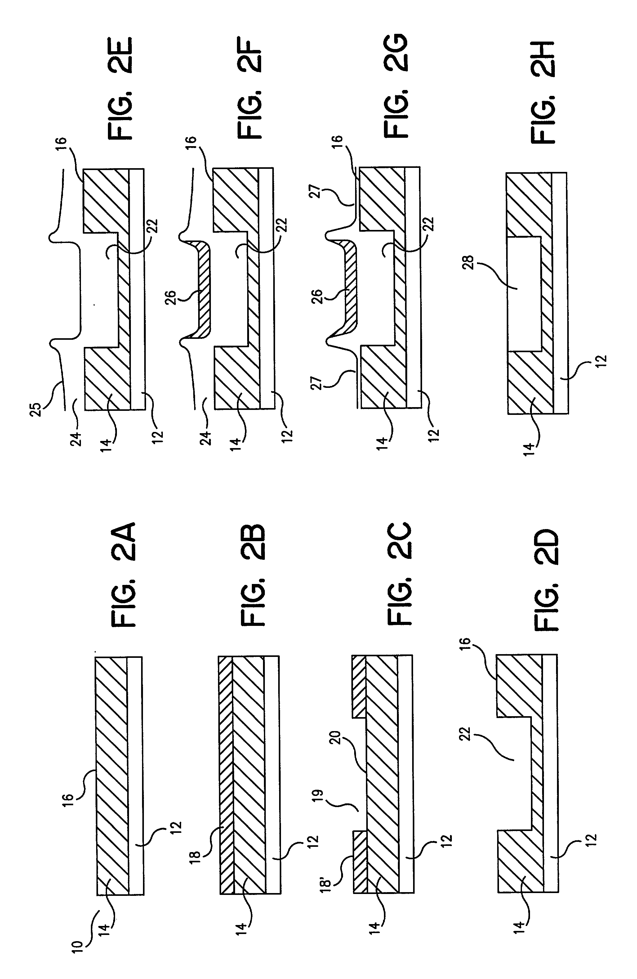
[0015] FIGS. 2A-2H are steps in one embodiment of processes of this invention for manufacturing substrates with large step-height features. In FIG. 2A, a substrate 10 is provided that includes a base material layer 12 and a first material layer 14 applied to the top of base material layer 12. First material layer 14 further includes an exposed surface 16. Typically, a feature, such as a large step height feature, a large width feature, a photonic li...
PUM
| Property | Measurement | Unit |
|---|---|---|
| Length | aaaaa | aaaaa |
| Height | aaaaa | aaaaa |
| Thickness | aaaaa | aaaaa |
Abstract
Description
Claims
Application Information
 - R&D
- Intellectual Property
- Life Sciences
- Materials
- Tech Scout
- Unparalleled Data Quality
- Higher Quality Content
- 60% Fewer Hallucinations
Browse by: Latest US Patents, China's latest patents, Technical Efficacy Thesaurus, Application Domain, Technology Topic, Popular Technical Reports.
© 2025 PatSnap. All rights reserved.Legal|Privacy policy|Modern Slavery Act Transparency Statement|Sitemap|About US| Contact US: help@patsnap.com