Detection system for chemical-mechanical planarization tool

a technology of chemical mechanical and planarization tool, which is applied in the direction of manufacturing tools, semiconductor/solid-state device testing/measurement, lapping machines, etc., can solve the problems of poor optical resolution of subsequent photolithography processing steps, both faces of the wafer to be extremely rough, and poor optical resolution of non-planar surfaces. , to achieve the effect of preventing the printing of high-density lines, poor optical resolution

Inactive Publication Date: 2005-02-03
NOVELLUS SYSTEMS
View PDF13 Cites 79 Cited by
  • Summary
  • Abstract
  • Description
  • Claims
  • Application Information

AI Technical Summary

Problems solved by technology

The slicing causes both faces of the wafer to be extremely rough.
Nonplanar surfaces create poor optical resolution of subsequent photolithography processing steps.
Poor optical resolution prohibits the printing of high-density lines.
Another problem with nonplanar surface topography is the step coverage of subsequent metallization layers.
If a step height is too large there is a serious danger that open circuits will be created.
Excessive removal of overburden from the front surface of the wafer, whether a raw sheet film, or an STI, metal or dielectric layer structure on the front wafer surface, may damage the wafer.

Method used


Image

  • Detection system for chemical-mechanical planarization tool
  • Detection system for chemical-mechanical planarization tool
  • Detection system for chemical-mechanical planarization tool

Examples


Embodiment Construction

[0022] The following detailed description is merely exemplary in nature and is not intended to limit the invention or the application and uses of the invention. Furthermore, there is no intention to be bound by any expressed or implied theory presented in the preceding technical field, background, brief summary or the following detailed description.

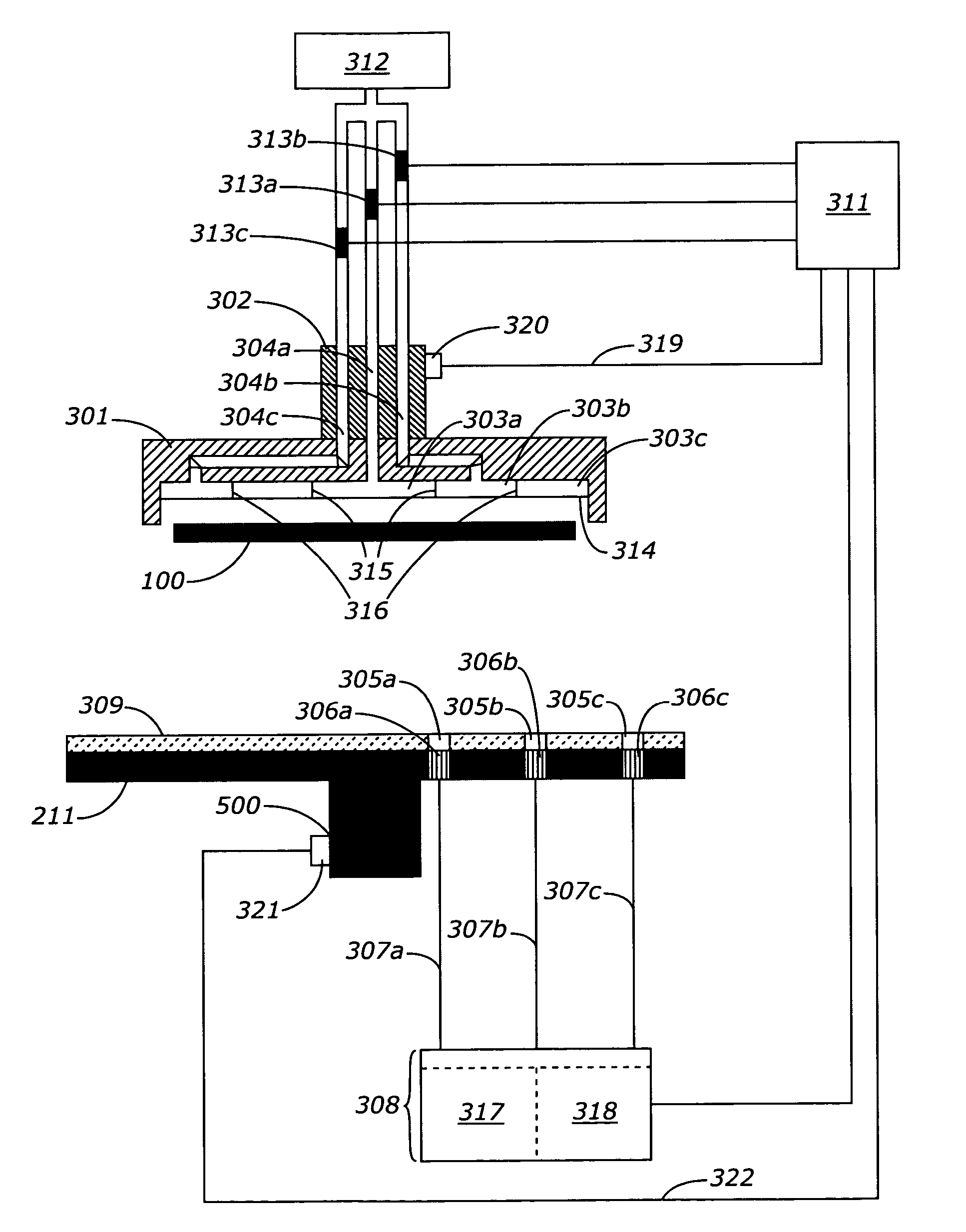
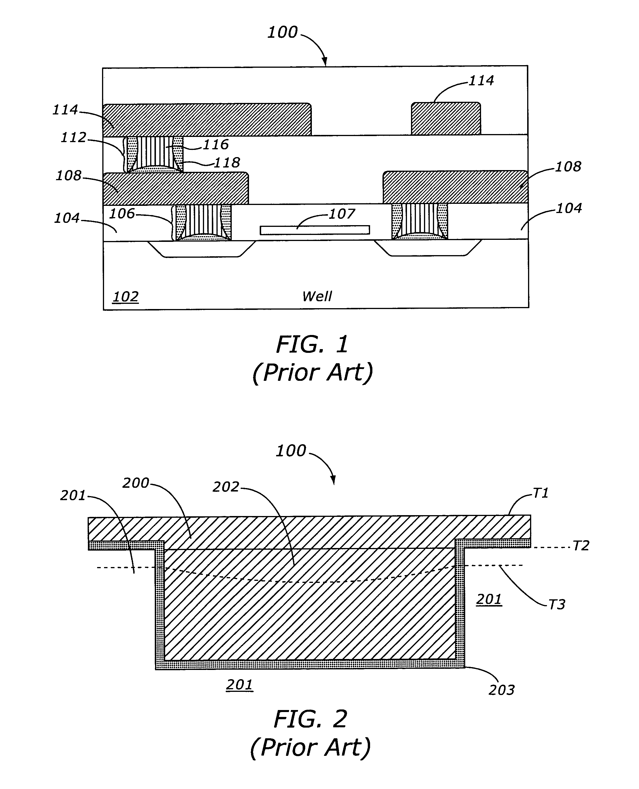
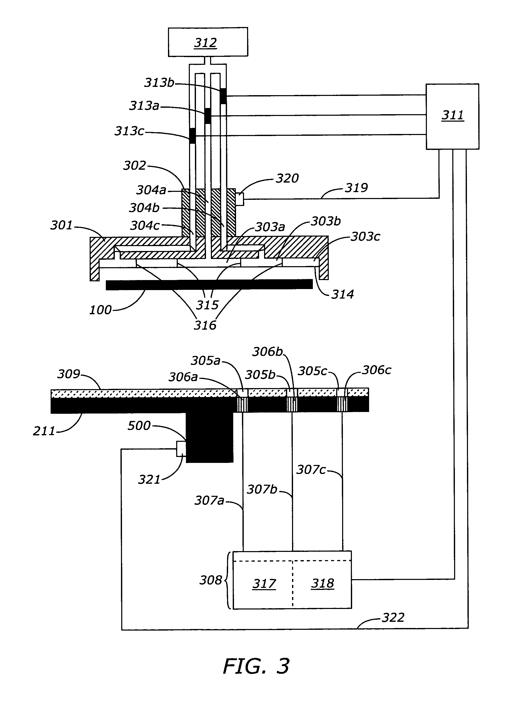
[0023] CMP of copper will become one of the most common and critical chemical mechanical planarization processes when the copper interconnect technology starts to dominate the fabrication of integrated circuits. FIG. 2 illustrates some of the potential problems if excessive overburden is removed, in this case a barrier layer 203, from the front surface of a wafer. At time T1 a layer of deposited copper 200 remains on the wafer. The copper layer is removed with a CMP step exposing barrier layer 203. In general, barrier layer 203 is deposited before copper 200. Barrier layer 203 forms a layer on the bottom and sidewalls of a cavity, via op...


PUM

PropertyMeasurementUnit
wavelengthaaaaaaaaaa

Abstract

Methods and apparatus are provided for endpoint detection in a chemical mechanical planarization (CMP) process. Reflectance spectra data is taken periodically in different areas of a surface of a semiconductor wafer during a chemical mechanical planarization process. Three different reflectance spectra are identified to determine a status of the CMP process. A first reflectance spectra data corresponds to light reflected predominately from a layer of material on the surface of the semiconductor wafer. A second reflectance spectra corresponds to the layer of material being thinned such that the second reflectance spectra is modified by an underlying layer of material. A third reflectance spectra corresponds to light reflected predominately from the underlying layer of material.

Description

TECHNICAL FIELD [0001] The present invention generally relates to the chemical mechanical planarization of semiconductor wafers, and more particularly relates to the detection of an end point of a chemical mechanical planarization process. BACKGROUND [0002] A flat disk or “wafer” of single crystal silicon is the basic substrate material in the semiconductor industry for the manufacture of integrated circuits. Semiconductor wafers are typically created by growing an elongated cylinder or boule of single crystal silicon and then slicing individual wafers from the cylinder. The slicing causes both faces of the wafer to be extremely rough. The front face of the wafer on which integrated circuitry is to be constructed must be extremely flat in order to facilitate reliable semiconductor junctions with subsequent layers of material applied to the wafer. Also, the material layers (deposited thin film layers usually made of metals for conductors or oxides for insulators) applied to the wafer...

Claims


Application Information

Patent Timeline
Patent Type & Authority Applications(United States)
IPC IPC(8): B24B1/00B24B37/04B24B49/00B24B49/12B24B51/00B24D7/12H01L21/66
CPCB24B37/013H01L22/26B24D7/12B24B49/12
Inventor BATTAL, TEZERLAURSEN, THOMAS
Owner NOVELLUS SYSTEMS
Why Eureka
Try Eureka