SRAM compatible and page accessible memory device using dram cells and method for operating the same

Inactive Publication Date: 2003-09-25
SILICON7
3 Cites 2 Cited by

AI-Extracted Technical Summary

Problems solved by technology

However, since the unit memory cell of the SRAM is implemented by six (6) transistors, it requires a larger space than that of the DRAM implemented by one (1) transistor and one (1) capacitor.
So, the manufacturing cost for the SRAM is increased, compared with the DRAM.
Therefore, the performance of the system itself may be deteriorated due to low-speed operation and the periodic refresh operation of the DRAM.
The memory device is compatible with a synchronous SRAM requiring exter...

Abstract

An SRAM compatible and page accessible memory device using DRAM cells, and a method for operating the same. The semiconductor memory device is implemented by DRAM cells and performs a refresh operation internally, but externally operates as a conventional SRAM. The semiconductor memory device includes a memory array; an address input unit for receiving word addresses and page addresses; an address detection unit generating a page address transition detection signal in response to a transition of at least one page address, and generating a word address transition detection signal in response to a transition of at least one word address; and a memory array control unit for controlling a page access operation of the memory array. The memory array control unit controls the semiconductor memory device to enter into a normal access state responsive to the page address transition detection signal, and controls the semiconductor memory device to perform the page access operation for changing the column selected by the column selection means in response to the word address transition detection signal, with maintaining the word line in the activation state.

Application Domain

Digital storageMemory systems

Technology Topic

Ip addressSemiconductor memory +6

Image

  • SRAM compatible and page accessible memory device using dram cells and method for operating the same
  • SRAM compatible and page accessible memory device using dram cells and method for operating the same
  • SRAM compatible and page accessible memory device using dram cells and method for operating the same

Examples

  • Experimental program(1)

Example

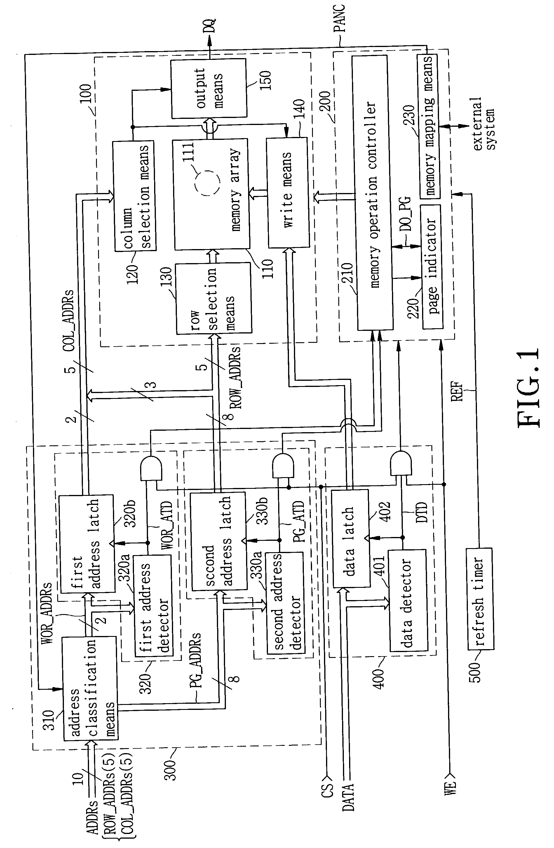
[0020] In a memory device according to the invention, DRAM cells are implemented and a refresh operation is performed internally. But, duration for the refresh operation is not allocated in operation specification like as the general SRAM. Also, the memory device of the invention externally operates as the conventional SRAM without requiring additional signals for controlling the refresh operation.
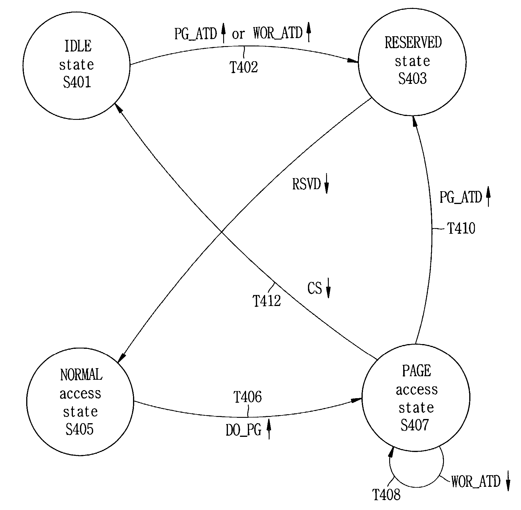
[0021] The memory device has several states including a REFRESH state, a RESERVED state, an ACCESS state and an IDLE state.
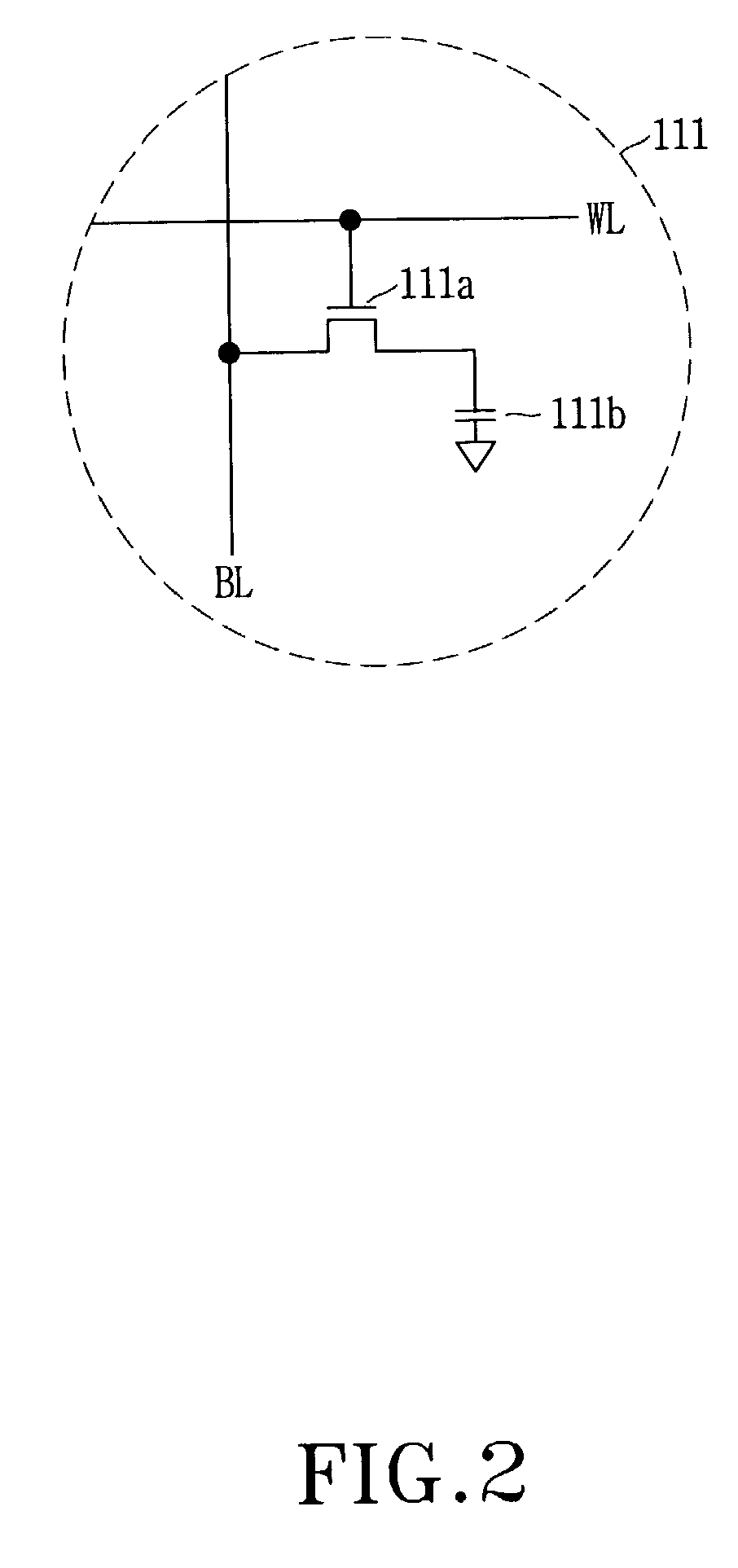
[0022] In the REFRESH state, the memory device activates a word line and reads out data from the memory cells connected to the activated word line. And then the data is amplified and restored to the memory cells.
[0023] In the RESERVED state, the REFRESH state can be allocated for the memory device. That is, the RESERVED state is transited into the REFRESH state, in response to a refresh operation signal provided from a refresh timer.
[0024] In the ACCESS state, write/read operations can be performed for the memory cells in the memory array. The ACCESS state includes a page (PAGE) access state. In the PAGE access state, a PAGE access operation can be performed. In the PAGE access operation, two or more columns can be successively selected by external input addresses and the data is read out or written, while the word line is maintained in the activated state. In the PAGE access operation, the access time can be reduced for the next access. The PAGE access state throughout the specification and claims means a state in which the word line is activated. On the other hand, for convenience of explanation, the other state of the ACCESS state except the PAGE access state is designated as a normal (NORMAL) access state.
[0025] In the IDLE state, a chip selection signal is not yet activated, so that the memory device itself is disabled.
[0026] FIG. 1 is a block diagram showing a semiconductor memory device according to one exemplary embodiment of the invention. The semiconductor memory device includes a data storing unit 100, a memory array controller 200, an address input unit 300, a data input unit 400 and a refresh timer 500.
[0027] The data storing unit 100 has a memory array 110 including a plurality of memory cells 111 arranged in a row and column type matrix. Each memory cell 111 requires the refresh operation for retention of data stored therein, within a predetermined refresh period. A DRAM cell is a typical example of the memory cell 111. Therefore, for convenience of explanation, the memory cell 111 is designated as a DRAM cell in this specification. As shown in FIG. 2, the DRAM cell can be implemented by a transfer transistor 111a to be gated by a word line (WL) and a capacitor 111b for storing data.
[0028] The address input unit 300 receives external input addresses (ADDRs), and classifies them as word addresses (WOR_ADDRs) and page addresses (PG_ADDRs). And, the address input unit 300 provides a word address transition detection signal (WOR_ATD) and a page address transition detection signal (PG_ATD) to the memory cell controller 200. The WOR_ATD is generated as a pulse in response to transition of the WOR_ADDRs, and the PG_ATD is generated as a pulse in response to transition of the PG_ADDRs.
[0029] Also, since the memory device of the invention operates as the conventional SRAM as above-mentioned, the address input unit 300 receives row selecting addresses and column selecting addresses at a substantially same time. Therefore, the row selecting addresses and the column selecting addresses are not externally classified. But, for convenience of explanation, the addresses selecting the row are designated as row selection addresses (ROW_ADDRs), and the addresses selecting the column are designated as column selection addresses (COL_ADDRs).
[0030] The address input unit 300 includes an address classification means 310, a word address detection means 320 and a page address detection means 330. The address classification means 310 classifies the ADDRs as the WOR_ADDRs and the PG_ADDRs. The WOR_ADDRs consist of a portion or all of the COL_ADDRs. The PG_ADDRs consist of the ROW_ADDRs and the remaining portion of the COL_ADDRs except the WOR_ADDRs. For example, if the memory device has 2.sup.5.times.2.sup.5 DRAM cells 111 and page depth of four (4), the number of each of the COL_ADDRs and the ROW_ADDRs is five (5) and the number of the ADDRs is ten (10). The page depth means the number of the PAGE access operations which are successively performed. Since the page depth is four (4), the number of the WOR_ADDRs is two (2), and the number of the PG_ADDRs is eight (8).
[0031] The word address detection means 320 detects the transition of the WOR_ADDRs, and transfers the WOR_ADDRs to a column selection means 120. The word address detection means 320 includes a first address detector 320a and a first address latch 320b. When the WOR_ADDR transition is detected, the first address detector 320a generates the WOR_ATD. Then, the WOR_ATD is provided to the memory array controller 200, when a chip selection signal (CS) is activated to a logic "high". The CS enables the memory device. The CS is externally provided. And, the first address latch 320b latches the WOR_ADDRs and supplies the same to the column selection means 120 in response to the WOR_ATD.
[0032] The page address detection means 330 detects the transition of the PG_ADDRs, and transfers the PG_ADDRs to the column selection means 120 and a row selection means 130. The page address detection means 330 includes a second address detector 330a and a second address latch 330b. The second address detector 330a generates the PG_ATD, when the PG_ADDRs' transition is detected. Then, the PG_ATD is provided to the memory array controller 200 when the CS is activated to a logic "high". And, the second address latch 330b latches the PG_ADDRs, and supplies the same to the column selection means 120 and the row selection means 130, in response to the PG_ATD. In this case, the PG_ADDRs, which are supplied to the column selection means 120, are not the WOR_ADDRs but the COL_ADDRs. And the PG_ADDRs, which are supplied to the row selection means 130, consist of the ROW_ADDRs.
[0033] Consequently, the COL_ADDRs are supplied to the column selection means 120, and the ROW_ADDRs are supplied to the row selection means 130.
[0034] In the embodiment shown in FIG. 1, ten (10) the ADDRs are classified as two (2) the WOR_ADDRs and eight (8) the PG_ADDRs, in the address classification means 310. But, the number of the WOR_ADDRs can be modulated, according to the page depth. For example, if the page depth is eight (8), the number of the WOR_ADDRs is modulated to three (3). In this case, the number of the WOR_ADDRs is controlled by a page depth control signal (PANC), which is provided from a memory mapping means 230 in the memory array controller 200.
[0035] The column selection means 120 decodes the COL_ADDRs, thereby selecting a column of the memory array 110. That is, the COL_ADDRs, which are decoded by the column selection means 120, control a write means 140 and an output means 150 so that the column of the memory array 110 is selected. And, the row selection means 130 decodes the ROW_ADDRs, thereby selecting a row of the memory array 110. That is, the ROW_ADDRs, which are decoded by the row selection means 130, activate a word line for the row to be selected, so that the row of the memory array 110 is selected.
[0036] The data input unit 400 receives an input data (DATA) and provides the received DATA to the write means 140. The data input unit 400 includes a data detector 401 and a data latch 402. The data detector 401 generates a data transition detection signal (DTD) when a DATA transition is detected. And, when the CS and a write enable signal (WE) are activated to a logic "high", the DTD is provided to the memory array controller 200. The WE controls the write/read operations of the memory device. When the WE is activated to a logic "high", the memory device of the invention is able to perform the write operation. On the other hand, when the WE is non-activated to a logic "low", the memory device is able to perform the read operation. The data latch 402 latches the DATA and supplies the same to the write means 140 in response to the DTD.
[0037] The DATA is latched by the data detector 401 and the data latch 402 so that the memory device is able to perform the PAGE access operation for the duration of the write (WRITE) operation, even if an additional control signal is not externally inputted.
[0038] The refresh timer 500 supplies the memory array controller 200 with a refresh request signal (REF) to be activated every predetermined refresh period, so that the DRAM cells 111 of the memory array 110 perform the refresh operation.
[0039] The memory array controller 200 includes a memory operation controller 210, a page indicator 220 and the memory mapping means 230.
[0040] The memory operation controller 210 controls operations of the memory array 110 such as the PAGE access operation and so forth. The page indicator 220 supplies a page indication signal (DO_PG) to the memory operation controller 210. The DO_PG is activated in a predetermined delay duration from generation of the PG_ATD or the WOR_ATD. The memory mapping means 230 communicates with an external system, and generates the PANC for controlling the page depth.
[0041] FIG. 3 is a timing diagram for explaining main signals generated during an access operation of the memory device. Referring to FIG. 3, the CS is logic "high" and the WE is logic "low". The PG_ATD is activated in response to the PG_ADDR transition, and the WOR_ATD is activated in response to the WOR_ADDR transition.
[0042] The DO_PG is activated in the delay duration from generation of the PG_ATD or the WOR_ATD. And, the DO_PG is non-activated to a logic "low" by the PG_ATD. Therefore, when the PG_ATD is activated, the DO_PG becomes non-activated with a predetermined pulse width and thereafter is activated again. And, when the WOR_ATD is activated in the activation state of the DO_PG, the DO_PG continuously holds the activation state.
[0043] FIG. 4 is a state transition diagram for explaining state transition in the memory device. In the state transition diagram shown in FIG. 4, entry into the other states or operation in the other states except the IDLE state S401 is described on the assumption that the CS is activated to a logic "high".
[0044] When either the PG_ATD or the WOR_ATD becomes activated to a logic "high" in the IDLE state S401, the memory device enters into the RESERVED state S403, at transition T402. Then, after a predetermined first duration from the entry into the RESERVED state S403 (that is, a reservation duration) (RSVD.dwnarw.), the memory device enters into the NORMAL access state S405, at transition T404. Preferably, the first duration is defined as a time interval to access the DRAM cell 111 of the memory array 110 from the entry into the NORMAL access state.
[0045] After a predetermined second duration from the NORMAL access state S405, the DO_PG becomes activated to a logic "high". Then, the memory device enters into the PAGE access state S407 responsive to activation of the DO_PG, at transition T406. The second duration means a time interval between the entry into the NORMAL access state S405 and the activation of a signal for driving the word line for selecting the row in the memory array 110.
[0046] In the PAGE access state S407, even if the WOR_ATD is activated to a logic "high", the memory device retains the PAGE access state S407, at transition T408. On the other hand, when the PG_ATD is activated to a logic "high" in the PAGE access state S407, the memory device returns to the RESERVED state S403, at transition T410. Also, when the CS is non-activated to a logic "low" in the PAGE access state S407, the memory device returns to the IDLE state S401, at transition T412.
[0047] According to the memory device and the method for operating the same in the invention, after the second duration from the entry into the NORMAL access state, the DO_PG is activated and then the memory device enters into the PAGE access state. And, even if the WOR_ADDRs are transited in the activation state of the DO_PG, the memory device performs the page access operation. Thereafter, when the PG_ADDRs are transited, the memory device returns to the RESERVED state again and performs the normal access operation.
[0048] While this invention has been particularly shown and described with reference to the embodiment thereof, it will be understood by those skilled in the art that various changes and equivalents may be made without departing from the spirit and scope of the invention. For example, in the embodiment, the RESERVED state being able to perform the refresh operation or the REFRESH state occurs before the read or the write operation. But, in another embodiment, it is obvious to those skilled in the art that the REFRESH state can occur after the read or the write operation. Therefore, it is intended that the invention not be limited to the particular embodiment disclosed as the best mode contemplated for carrying out this invention, but that the invention will include all embodiments within the scope of the appended claims.

PUM

no PUM

Description & Claims & Application Information

We can also present the details of the Description, Claims and Application information to help users get a comprehensive understanding of the technical details of the patent, such as background art, summary of invention, brief description of drawings, description of embodiments, and other original content. On the other hand, users can also determine the specific scope of protection of the technology through the list of claims; as well as understand the changes in the life cycle of the technology with the presentation of the patent timeline. Login to view more.
Why Eureka
Try Eureka