Method and apparatus for measuring dopant profile of a semiconductor

a technology of semiconductor and dopant profile, which is applied in the direction of semiconductor/solid-state device testing/measurement, instrumentation, individual semiconductor device testing, etc., can solve the problems that all prior art techniques generally do not have a very high sensitivity and/or spatial resolution to meet the demands of integrated circuit manufacturing at submicron levels, and the sensitivity of some prior art techniques tends to decreas

Inactive Publication Date: 2003-10-02
IBM CORP
View PDF0 Cites 13 Cited by
  • Summary
  • Abstract
  • Description
  • Claims
  • Application Information

AI Technical Summary

Problems solved by technology

However, all of the prior art techniques generally do not have a very high sensitivity and / or spatial resolution to meet the demands of integrated circuit manufacturing at submicron levels.
Furthermore, the sensitivity of some of the prior art techniques tends to decrease as the spatial resolution increases with the usage of sharper probes.

Method used


Image

  • Method and apparatus for measuring dopant profile of a semiconductor
  • Method and apparatus for measuring dopant profile of a semiconductor
  • Method and apparatus for measuring dopant profile of a semiconductor

Examples


Embodiment Construction

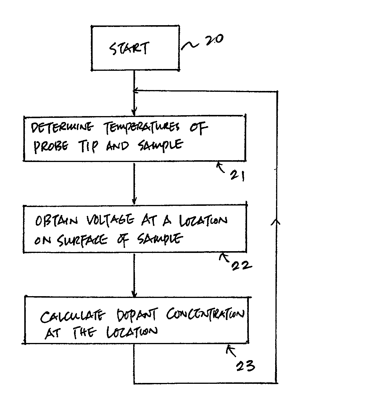
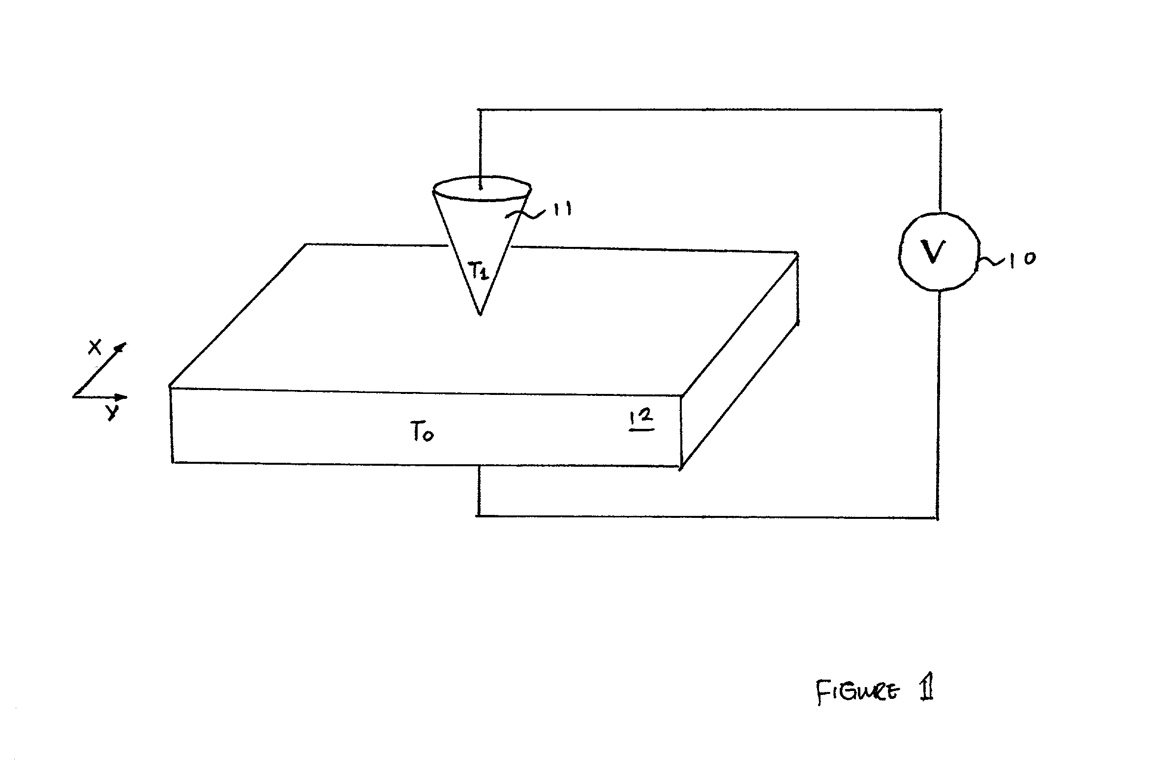
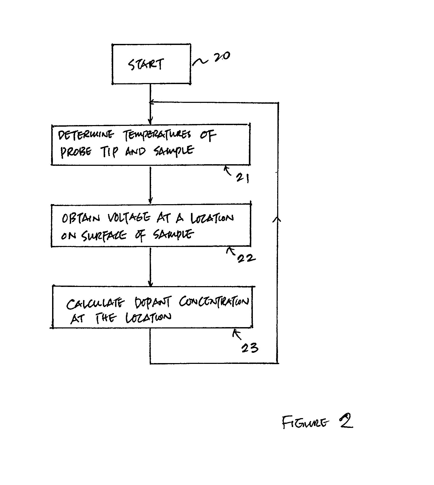
[0013] The Seebeck coefficient of a semiconductor depends on the concentration of dopants within the semiconductor. For example, the Seebeck coefficient S of an n-type silicon is 1S = 1 - e T ( E C - E F + 2 k B T ) - k B eln n N c

[0014] where

[0015] e=charge

[0016] T=temperature

[0017] n=dopant concentration

[0018] E.sub.C=conduction band energy

[0019] E.sub.F=Fermi energy

[0020] k.sub.B=Boltzman constant

[0021] N.sub.c=constant

[0022] Thus, the dopant concentration of a semiconductor can be determined by measuring the Seebeck coefficient of the semiconductor via 2 n = N cexp [ - eS k B]

[0023] The Seebeck coefficient can be measured by using Scanning Thermoelectric Microscopy (STEM), as detailed in Ghoshal, Miner and Majumdar, Proc. 19.sup.th, Int. Thermoelectrics Conference, p. 221 (2000), the pertinent of which is incorporated herein by reference, or Scanning Chemical Potential Microscopy (SCPM), as detailed in Williams and Wickramasinghe, Nature, 344, p. 317 (1990), the pertinent of whi...


PUM

PropertyMeasurementUnit
thermoelectric voltageaaaaaaaaaa
channel lengthaaaaaaaaaa
concentrationaaaaaaaaaa

Abstract

A method and apparatus for measuring dopant profile of a semiconductor is disclosed. Initially, the temperature of a tip of a probe and the temperature of a semiconductor sample are ascertained. Then, a voltage at a location on a surface of the semiconductor sample is obtained via the tip of the probe. The dopant concentration at the location of the surface of the semiconductor sample is subsequently determined by combining the obtained voltage and the temperature difference between the probe tip and the semiconductor sample. The above-mentioned steps can be repeated in order to generate a dopant profile of the semiconductor.

Description

[0001] 1. Technical Field[0002] The present invention relates to semiconductor characterization in general, and in particular to a method and apparatus for measuring the dopant profile of a semiconductor. Still more particularly, the present invention relates to a method and apparatus for measuring a two-dimensional dopant profile of a semiconductor.[0003] 2. Description of the Prior Art[0004] Present-day integrated circuit manufacturing technology demands accurate knowledge of the concentration of dopants that have been incorporated into substrates. This is because dopant concentration within a substrate has a significant effect on the performance of discrete devices, such as transistors, that are built on the substrate. In addition, it is also important to have the knowledge of the dopant concentration in a spatial extent for process development.[0005] Typically, the active region of a field-effect transistor (FET) is engineered by incorporating dopants, such as arsenic, boron, or...

Claims


Application Information

Patent Timeline
Patent Type & Authority Applications(United States)
IPC IPC(8): G01Q10/06G01N27/00G01Q60/00
CPCY10S977/854G01N27/002
Inventor SHI, LIGHOSHAL, UTTAM SHYAMALINDU
Owner IBM CORP
Why Eureka
Try Eureka