

Transparent conductive laminate and process of producing the same
a technology of transparent conductive laminates and conductive layers, which is applied in the direction of conductive layers on insulating supports, instruments, applications, etc., can solve the problems of poor film transparency, large change in resistivity after wet heat test, and inability to fabricate films at high temperature, etc., to achieve excellent transparency, reduce the effect of carrier density and two-times higher hall mobility
- Summary
- Abstract
- Description
- Claims
- Application Information
AI Technical Summary
Benefits of technology
Problems solved by technology
Method used
Image

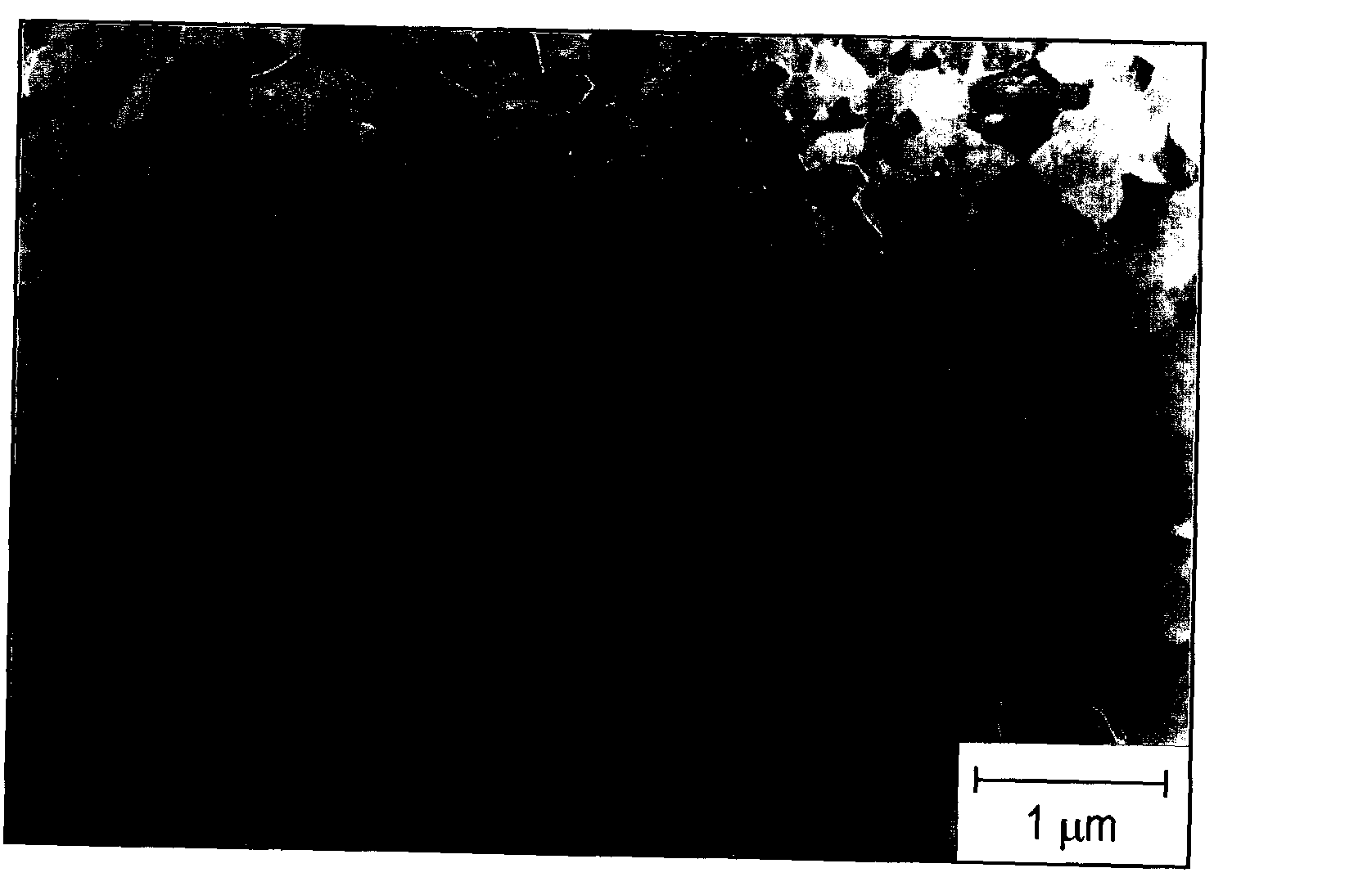
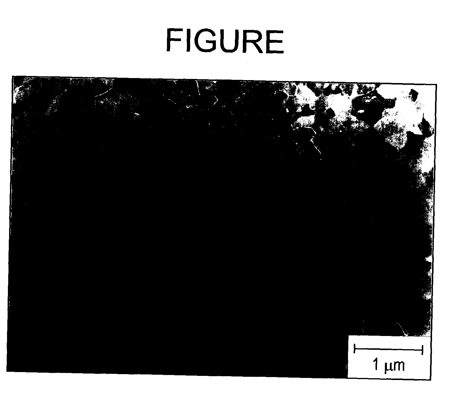
Examples
example 2
[0044] An In--Sn oxide target (amount of Sn atom: 4.7% by weight based on the total weight of In atom and Sn atom) as a target material and a PET film having a thickness of 75 .mu.m as a substrate were installed in a rolling up-type magnetron sputtering device of parallel plate type. The device was subjected to dehydration and degassing and evacuated to a degree of vacuum of 1.times.10.sup.-4 Pa while rolling up.
[0045] In this state, sputter film formation was carried out in a reactive sputtering process with a 3 kW DC by introducing 300 seem of an Ar gas by heating at a substrate temperature of 100.degree. C. and by setting a plasma emission intensity of In by only the Ar gas at 90 and then regulating an amount of an oxygen gas introduced while opening and closing an automatic piezo valve such that the emission intensity after the introduction of oxygen gas became 86 by PEM, to adjust the film quality.
[0046] There was thus formed a 20 nm-thick transparent conductive layer made of a...
PUM
| Property | Measurement | Unit |
|---|---|---|
| thickness | aaaaa | aaaaa |
| thickness | aaaaa | aaaaa |
| temperature | aaaaa | aaaaa |
Abstract
Description
Claims
Application Information