
Use of a U-groove as an alternative to using a V-groove for protecting silicon against dicing induced damage

a technology of dicing and u-groove, which is applied in the direction of cable/conductor manufacturing, electrical equipment, manufacturing tools, etc., can solve the problems of increasing the complexity and cost of the system, increasing the complexity of the system, and single or multiple die combinations such as described above usually require more complex and expensive optical systems, so as to achieve tight dicing accuracy and high resolution. , the effect of improving the dicing accuracy

Inactive Publication Date: 2003-10-16
XEROX CORP
View PDF8 Cites 3 Cited by
  • Summary
  • Abstract
  • Description
  • Claims
  • Application Information

AI Technical Summary

Benefits of technology

[0004] However, a long or full width array, having a length equal to or larger than the document line and with a large packing of co-linear photo-sites to assure high resolution, has been and remains a very desirable arrangement. In the pursuit of a long or full width array, forming the array by assembling several small dies together end to end has become an exemplary arrangement. However, this necessitates providing dies whose photo-sites extend to the border or edge of the die, so as to assure continuity when the die is assembled end to end with other dies, and at the same time provide edges that are sufficiently smooth and straight to be assembled together without loss of image data.
[0005] Although the standard technique of scribing and cleaving silicon wafers used by the semiconductor industry for many years produces dies having reasonably controlled dimensions, the microscopic damage occurring to the die surface during the scribing operation has effectively precluded the disposition of the photo-sites at the die edge. This is because the top surface of silicon wafers is virtually always parallel to the <100> plane of the crystalline lattice so that, when a wafer of this type is cut or diced with a high speed diamond blade, chips and slivers are broken away from the top surface of the wafer in the direct vicinity of the channel created by the blade. This surface chipping typically extends to about 50 microns, thus, rendering it impossible for active elements to be located any closer than about 50 microns from the dicing channel. This as a result, has driven the adoption of V-shaped grooves as a technique for providing much smoother dicing and thereby enabled tighter dicing accuracy and closer proximity of active chip elements to the chip / die edge.
[0008] Therefore, as discussed above, there exists a need for an arrangement and methodology which will solve the problem of preventing cracks and chipping caused by damage from sawing while minimizing the costs of doing so. Thus, it would be desirable to solve this and other deficiencies and disadvantages as discussed above with an improved semiconductor dicing methodology.
[0011] The present invention also relates to a method of fabricating high resolution image sensor dies from a wafer so that the dies have precision faces to enable the dies to be assembled with other like dies to form a larger array without image loss or distortion at the points where the dies are assembled together. The method comprising the steps of etching small U-shaped grooves in one side of a wafer delineating the faces of the dies where the dies are to be separated from the wafer. This is followed by forming grooves in the opposite side of the wafer opposite each of the U-shaped grooves, the axis of the grooves being parallel to the axis of the U-shaped groove opposite thereto. In turn this is followed by, sawing the wafer along the U-shaped grooves with one side of the cut made by sawing being substantially coextensive with the bottom of the U-shaped grooves whereby one side of the U-shaped grooves is at least partially obliterated by the sawing, the sides of the U-shaped grooves that remain serving to prevent development of fractures in the die beyond the remaining side as the wafer is being sawed.

Problems solved by technology

Because of the difficulty in economically designing and fabricating long dies, image resolution for the typical die commercially available today is relatively low when the die is used to scan a full line.
While resolution may be improved electronically as by interpolating extra image signals, or by interlacing several smaller dies with one another in a non-collinear fashion so as to crossover from one die to the next as scanning along the line progresses, electronic manipulations of this type adds to both the complexity and the cost of the system.
Further, single or multiple die combinations such as described above usually require more complex and expensive optical systems.
Although the standard technique of scribing and cleaving silicon wafers used by the semiconductor industry for many years produces dies having reasonably controlled dimensions, the microscopic damage occurring to the die surface during the scribing operation has effectively precluded the disposition of the photo-sites at the die edge.
This surface chipping typically extends to about 50 microns, thus, rendering it impossible for active elements to be located any closer than about 50 microns from the dicing channel.
However, utilization of a V-shaped groove technique while effective has proven to be expensive.
First, there are the extra foundry costs.
This also means that the wafers must be stripped of their photoresist and require extra handling with placement in an off-line wet etch tool as well.
Secondly, there is the cost impact resulting from chip yield effects.
Anisotropic etching is by nature an aggressive etch due to the chemicals employed and, thus, often attacks and damages the top layers of passivation oxide and metal on the wafer.

Method used


Image

  • Use of a U-groove as an alternative to using a V-groove for protecting silicon against dicing induced damage
  • Use of a U-groove as an alternative to using a V-groove for protecting silicon against dicing induced damage
  • Use of a U-groove as an alternative to using a V-groove for protecting silicon against dicing induced damage

Examples


Embodiment Construction

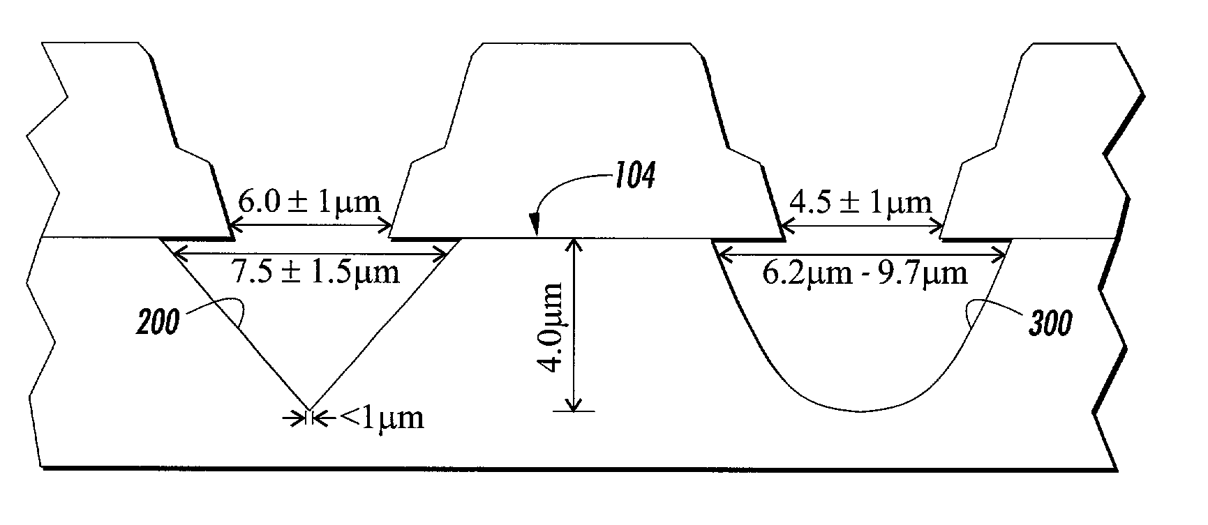
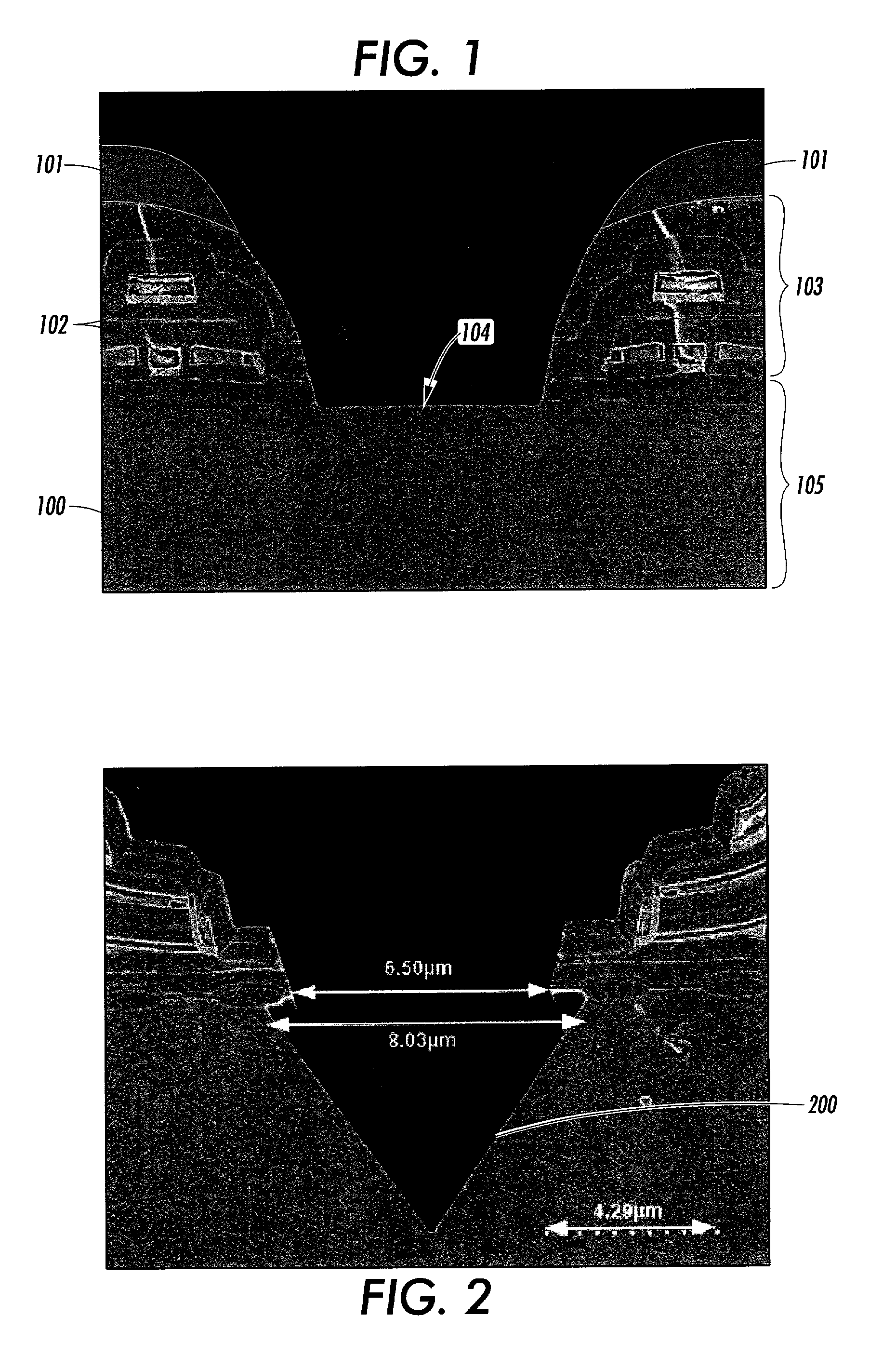
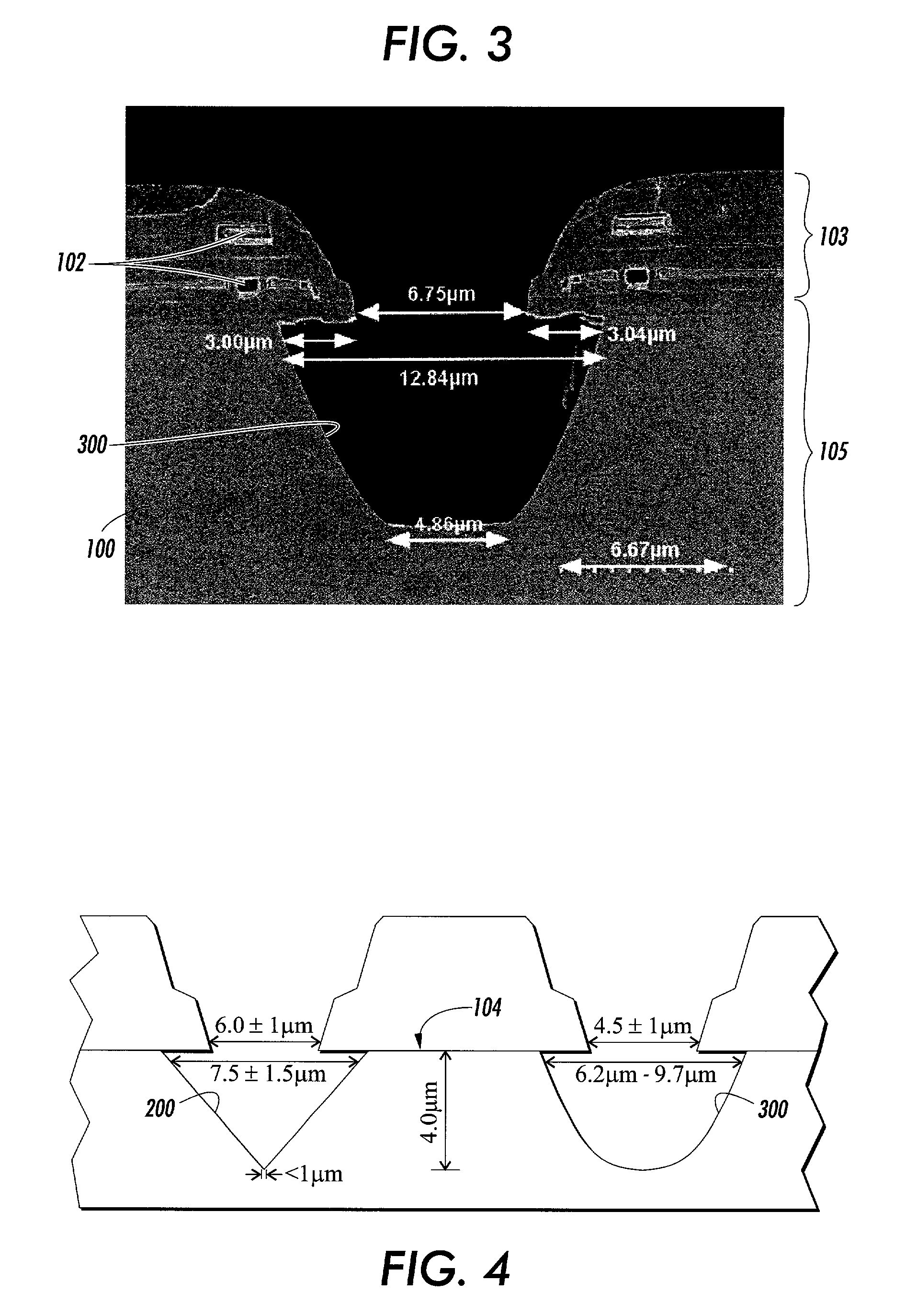
[0016] The prior approach employed of using a V-groove for dicing image sensor dies as described above has associated with it increased costs, process cycle time, reduced yield and increased metal layer defects. The disclosure taught herein overcomes these disadvantages by replacing the V-groove with a U-groove, using in one embodiment a dry etch consisting of SF.sub.6, He and O.sub.2. The intent of etching a V-groove into the silicon is to relieve damage to the device caused by dicing the wafer. A U-groove has proven itself as an improvement because the angle of the U-groove is sufficient to deflect cracking and stress away from the device while only requiring a dry etch for its achievement.

[0017] FIG. 1 depicts a cross section of a wafer 100 comprising dies to be diced. The cross section depicted is a SEM magnification of one dicing channel on wafer 100. Here in FIG. 1 is depicted the result after photoresist 101 has been applied, exposed, and developed, and with a subsequent firs...


PUM


Abstract

The present disclosure relates that by modifying chip die dicing methodology to a U-groove profile from a V-groove profile by modifying the second etch step to be a dry etch instead of a wet etch results in a direct cost savings by eliminating a more expensive process step, as well as the need for stripping the developed photoresist layer. Furthermore, going to a U-groove profile accomplishes additional indirect and greater cost savings resulting from increased process throughput, improved yield, and reduced metal layer defects.

Description

BACKGROUND OF THE INVENTION AND MATERIAL DISCLOSURE STATEMENT[0001] The present invention relates generally to the fabrication of semiconductor devices. In particular, to the dicing of integrated circuit chips with great accuracy, and within close proximity to fabricated elements on the chip. The invention relates, most particularly, to the dicing of silicon sensor chips as employed for digital image sensors.[0002] Image sensor dies for scanning document images, such as Charge Coupled Devices (CCDs), typically have a row or linear array of photo-sites together with suitable supporting circuitry integrated onto silicon. Usually, a die of this type is used to scan line by line across the width of a document with the document being moved or stepped lengthwise in synchronism therewith.[0003] In the above application, the image resolution is proportional to the ratio of the scan width and the number of array photo-sites. Because of the difficulty in economically designing and fabricating...

Claims


Application Information

Patent Timeline
IPC IPC(8): B28D5/02H01L21/301H01L21/3065
CPCH01L21/78B28D5/022
Inventor PERREGAUX, ALAIN E.HOSIER, PAUL A.JEDLICKA, JOSEF E.SALATINO, NICHOLAS J.TANDON, JAGDISH C.
Owner XEROX CORP
Learn More