Second level packaging interconnection method with improved thermal and reliability performance

US20030202332A1Inactive Publication Date: 2003-10-30NOKIA CORP

Image

  • Second level packaging interconnection method with improved thermal and reliability performance
  • Second level packaging interconnection method with improved thermal and reliability performance
  • Second level packaging interconnection method with improved thermal and reliability performance

Examples


Embodiment Construction

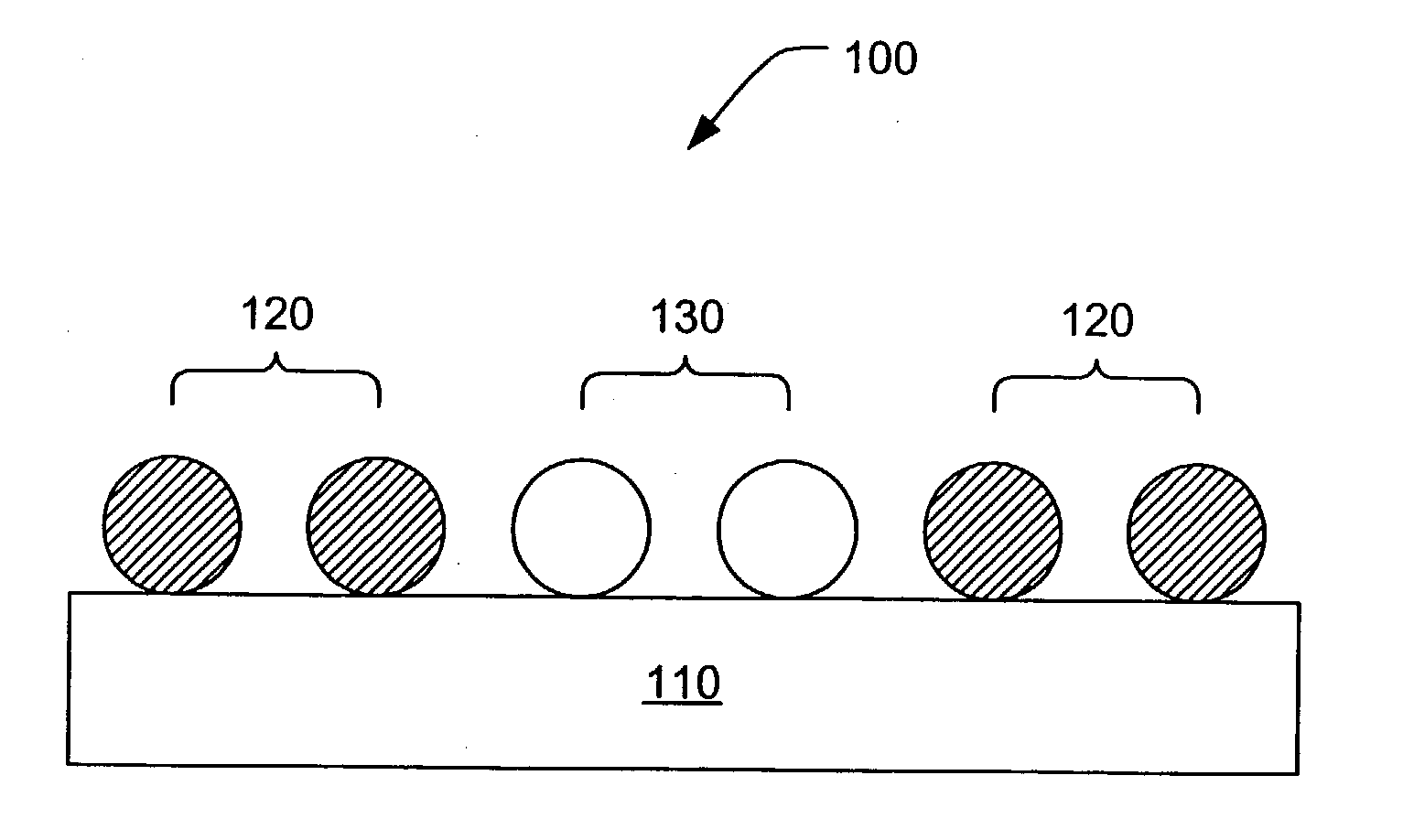
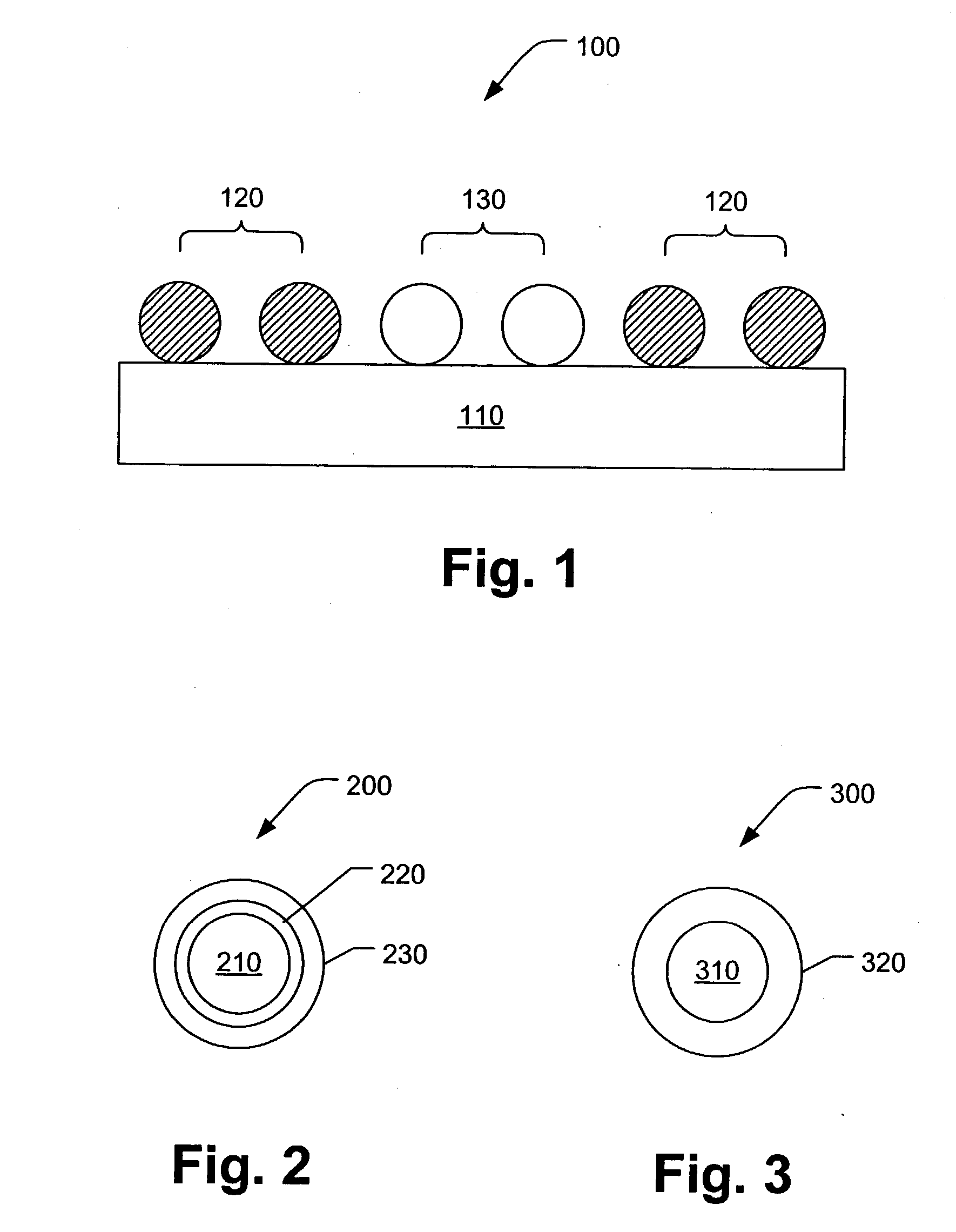
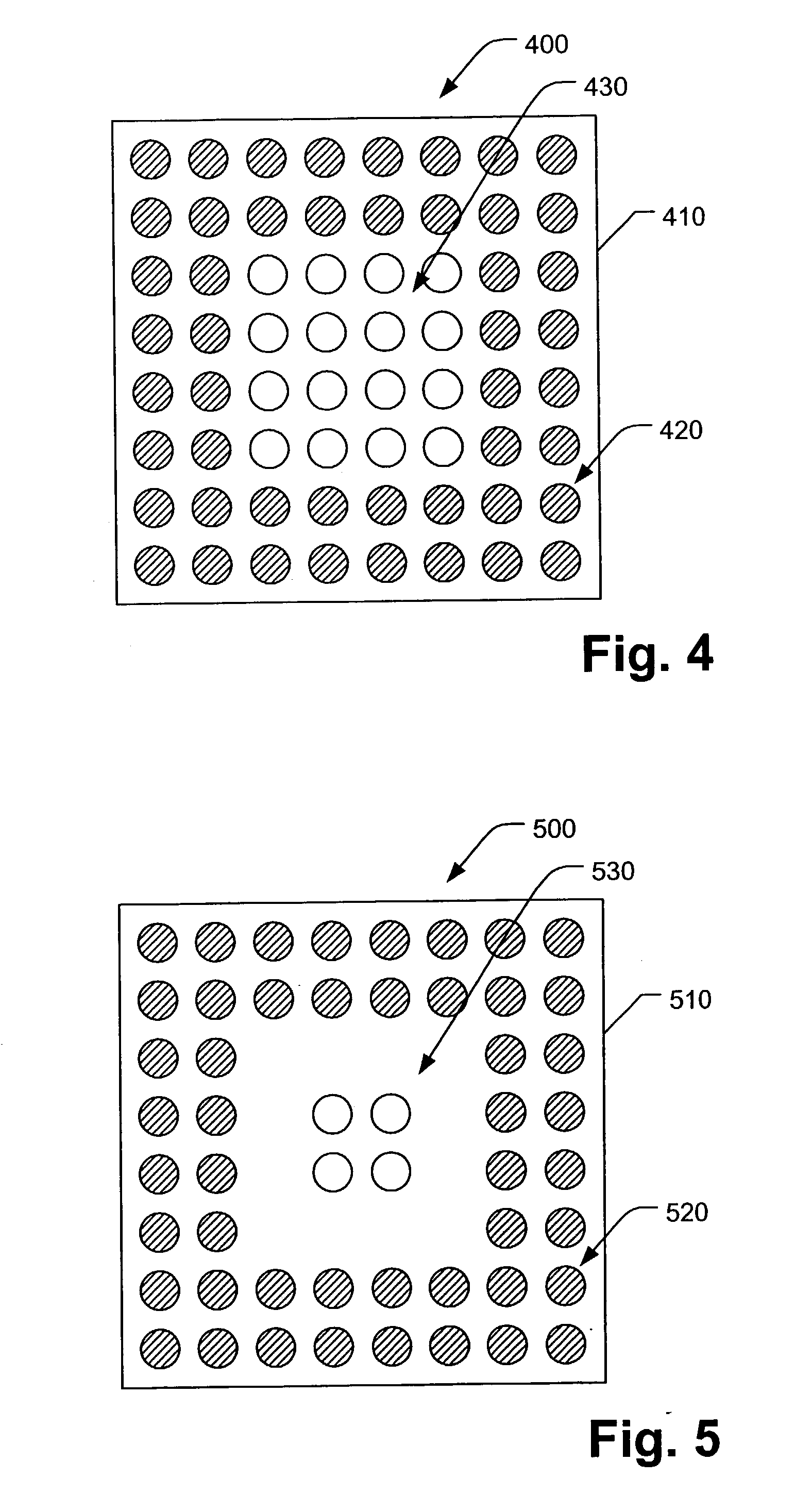
[0020] The present invention relates to second level packaging in electronics, e.g., interconnects between a package, containing an IC chip, such as an Application Specific Integrated Circuit (ASIC), a memory, or any combination of chips, and a printed wiring board; and will now be described with reference to the drawings, wherein like reference numerals are used to refer to like elements throughout. In the following description, for purposes of explanation, numerous specific details are set forth in order to provide a thorough understanding of the present invention. It may be evident, however, that the present invention may be practiced without these specific details. In other instances, well-known structures and devices are shown in block form in order to facilitate describing the present invention.

[0021] Second level packaging involves integrated circuit packages and other components being assembled onto substrates, such as printed wiring boards and ceramic substrates. The integr...


PUM


Abstract

Surface mount packages having a plurality of polymer and metallic contacts (e.g., balls) applied thereon and methods of fabricating and utilizing such packages are provided. The polymer balls are employed to improve mechanical compliance of the package; and the metallic (e.g., copper) balls are employed to improve thermal conduction between the package and a substrate to which the package is attached. The polymer balls can be located on a periphery portion of a package where mechanical and thermal stresses are the highest; and the metallic balls can be located on a middle portion of the package. Thus the present invention improves both mechanical stresses and thermal conductivity of a second level packaging interconnection, which in turn improves reliability of an electronic device.

Description

[0001] This application claims priority under 35 U.S.C. 119(e) to provisional application U.S. Serial No. 60 / 376,133 filed on Apr. 29, 2002.[0002] The present invention relates to second level packaging and, more particularly, to methods of fabricating and utilizing second level interconnects with improved thermal and reliability performance.[0003] Microelectronic devices contain millions of electrical circuit components, mainly transistors assembled in integrated circuit (IC) chips, but also resistors, capacitors, and other components. These chips are mounted on carriers or substrates, such as printed wiring boards, which physically support the chips and electrically interconnect the chips with other elements of the circuit. The interconnection between the chip itself and its supporting substrate is commonly referred to as a "first level" assembly or chip interconnection. This is distinguished from the interconnection between the substrate and larger elements of the circuit, which ...

Claims


Application Information

Patent Timeline
30 Oct 2003
Publication
US20030202332A1
IPC
H01L23/498; H05K3/34
CPC
H01L23/49816; H01L23/49838; H05K3/3436; H05K2201/0212; H05K2201/094; H01L2924/0002; H05K2201/10234; H01L2924/00
Inventors
REINIKAINEN, TOMMI; MYLLYKOSKI, PIRKKA