Multilayer laser trim interconnect method

a laser trim and interconnect technology, applied in the direction of semiconductor/solid-state device details, semiconductor devices, electrical equipment, etc., can solve the problems of increasing complexity and shrinking of semiconductor devices, increasing the footprint of packages, and increasing the complexity of semiconductor devices

Inactive Publication Date: 2004-01-22
TEXAS INSTR INC
View PDF3 Cites 60 Cited by
  • Summary
  • Abstract
  • Description
  • Claims
  • Application Information

AI Technical Summary

Benefits of technology

0022] The problems noted above are solved in large part by a method of creating electrical interconnects between a die and package without the use of wirebonds. Without wirebonds, the problems discussed above are eliminated or at least ameliorated to a great extent. Accordingly, the preferred method is to electrically connect a die and package substrate by applying an electrically non-conducting material over a die, extending onto the package substrate, and leaving a portion of the substrate contact pads exposed. An electrically conductive material is then applied over the non-conductive layer, coming into electrical contact with the die preferably by flowing into holes formed in the insulating layer over the die bond pads or by contacting conductive bumps which are formed on the die bond pads and protrude through the insulating layer. Portions of the conductive layer are then selectively removed to form conductive patches between electrical points of contact on the die and substrate contact pads, respectively. Further, the preferred method entails spraying a layer of conductive ink over an insulating epoxy or polyimide layer, then laser trimming the conductive ink layer to create separate connection traces.

Problems solved by technology

As semiconductor devices increase in complexity and shrink in size, packaging them is becoming more and more challenging as a greater numbers of electrical signals and other connections, such as grounds, have to be routed from increasingly smaller chips.
Several issues exist with peripherally leaded packages.
For instance, as all the signals on the die must be routed out the edge of the package, as pin count increases, the footprint of the package may be undesirably forced to increase geometrically since the package area is not utilized for interconnects.
For this reason, small increases in the pin count of the die can cause relatively large increases in overall package area, since exceeding the number of pins in one package size would force the die into the next larger package family.
Further, a myriad of issues exists with wirebonding, the default interconnect method used with leadframe packages.
For a fine-pitch die, or a die that requires a wire pitch smaller than current high-volume industry standards, and thus, requires a special wirebonder and thinner wires 32, the issue of wire sweep becomes even more troublesome.
Wire sag is also an issue with relatively long or thin wires, which have an inherent sag under their own weight due to their extremely small cross-sections.
For small products, such as cell phones or other popular mobile devices, any added semiconductor package height is undesired.
While area array packaging has met many packaging challenges, the practice of wirebonding still limits the capabilities and features of a packaged device.
However, the flipchip process is technically intricate and comparatively expensive, since the bump array on the substrate surface must exactly match that of the die.
Also, there is little wiring flexibility, and bumps are difficult to apply to fine-pitch die.
These custom, exclusive-use substrates often do not achieve the manufacturing volumes of more generic packaging means, and consequently can be much more expensive.

Method used


Image

  • Multilayer laser trim interconnect method
  • Multilayer laser trim interconnect method
  • Multilayer laser trim interconnect method

Examples


Embodiment Construction

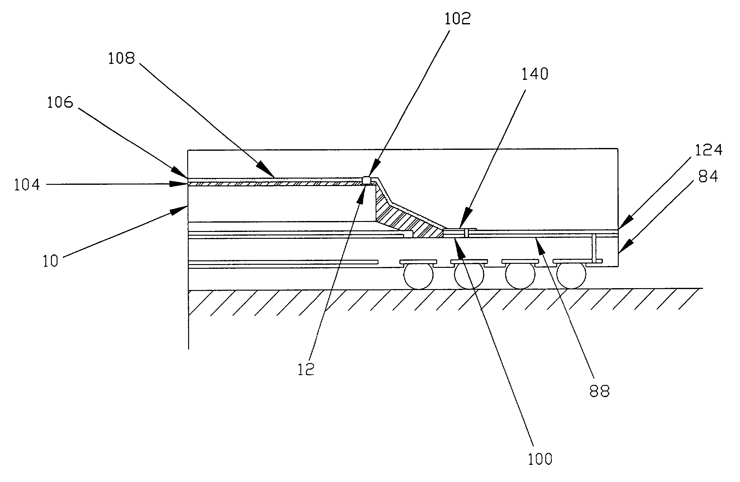
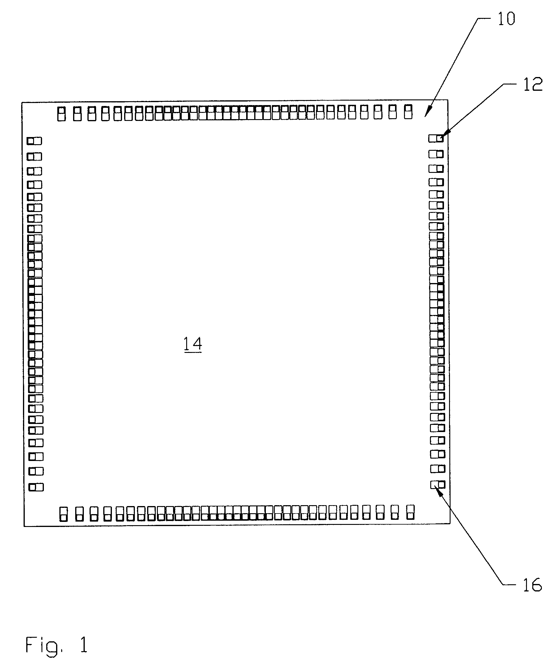
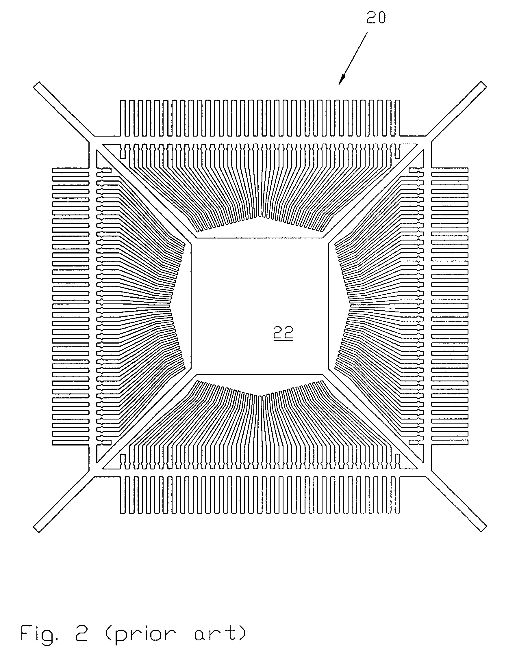
[0022] The problems noted above are solved in large part by a method of creating electrical interconnects between a die and package without the use of wirebonds. Without wirebonds, the problems discussed above are eliminated or at least ameliorated to a great extent. Accordingly, the preferred method is to electrically connect a die and package substrate by applying an electrically non-conducting material over a die, extending onto the package substrate, and leaving a portion of the substrate contact pads exposed. An electrically conductive material is then applied over the non-conductive layer, coming into electrical contact with the die preferably by flowing into holes formed in the insulating layer over the die bond pads or by contacting conductive bumps which are formed on the die bond pads and protrude through the insulating layer. Portions of the conductive layer are then selectively removed to form conductive patches between electrical points of contact on the die and substra...


PUM


Abstract

A method for creating electrical interconnects between a semiconductor die and package. In the preferred embodiment, an insulating material is applied over the die and extends to the substrate contact pads, leaving a portion of each contact pad exposed. Holes are then trimmed through the insulating material, exposing at least a portion of each die bond pad. A conductive material is then applied over the die, flowing into the holes, contacting the die bond pads, and extending out to contact at least a portion of each substrate contact pad. In another preferred embodiment, an electrically conductive bump may be formed on each die bond pad, protruding through said non-conductive material and at least partially through said conductive material. The conductive layer is then laser trimmed, forming conductive patches that serve as electrical interconnects between the die and package substrate.

Description

[0001] Not applicable.[0002] Not applicable.[0003] 1. Field of the Invention[0004] The present invention generally relates to a method for semiconductor packaging and assembly, and in particular to a method for creating improved interconnections between a die and package substrate. Still more particularly, the invention relates to a method for creating interconnects with subsequent layers of insulating and conductive materials.[0005] 2. Background Information[0006] Modern-day semiconductor devices, commonly called microchips, or "die," are fabricated on wafers, and the wafers are then sawn into grids, separating the individual chips prior to assembly in a package. Chips are fabricated in a variety of sizes, but typically range from only a few millimeters to a couple of centimeters or more in width. Each chip has numerous electrical signals. Processors, for example, may have several hundred signals. Provisions must be made to electrically connect a die to the component with which it ...

Claims


Application Information

Patent Timeline
Patent Type & Authority Applications(United States)
IPC IPC(8): H01L21/60H01L23/538
CPCH01L23/5389H01L24/11H01L2224/82007H01L2924/014H01L2924/01033H01L2924/01005H01L2224/32245H01L2224/32225H01L24/49H01L24/48H01L2924/15311H01L2924/01082H01L2224/73267H01L2224/73265H01L2224/49171H01L2224/48465H01L2224/48247H01L2224/48227H01L2224/48091H01L2224/4809H01L2224/24998H01L2224/24226H01L2224/24051H01L2224/13099H01L24/25H01L24/24H01L2924/00015H01L2924/00014H01L2924/00011H01L2924/00H01L2224/05554H01L2224/05599H01L2224/06135H01L2224/45099H01L2224/85399H01L2924/12042H01L2924/181H01L2924/00012H01L2224/45015H01L2924/207
Inventor NAKANISHI, NOBORU
Owner TEXAS INSTR INC
Why Eureka
Try Eureka