Electronic circuit, electronic device, electro-optical device, and electronic apparatus

a technology of electrooptical devices and electronic circuits, applied in static indicating devices, instruments, solid-state devices, etc., can solve problems such as remarkable problems, delay in recording the operation of data current in the pixel circuit, and delay in operation

Active Publication Date: 2004-02-26
ELEMENT CAPITAL COMMERCIAL CO PTE LTD
View PDF13 Cites 6 Cited by
  • Summary
  • Abstract
  • Description
  • Claims
  • Application Information

AI Technical Summary

Benefits of technology

[0017] Accordingly, it is possible to accurately input the input signal to the first circuit and the second circuit by alternately inputting the input signal to the first circuit and the second circuit forming the buffer circuit. Also, it is possible to use a period where any one of the first circuit and the second circuit receives the input signal as a period where the other circuit performs an output to the second signal line.
[0019] Accordingly, it is possible to accurately output the output signal corresponding to the input signal by alternately outputting an output signal from the first circuit and the second circuit. Also, it is possible to use a period where any one of the first circuit and the second circuit performs an output for the second signal line as a period where the other circuit receives the input signal. Accordingly, it is possible to effectively use time.
[0021] Accordingly, it is possible to form the buffer circuit by a simple circuit. Therefore, it is possible to reduce the size of the buffer circuit.
[0023] Accordingly, it is possible to form the buffer circuit by a simple circuit. Therefore, it is possible to reduce the size of the buffer circuit.
[0025] Accordingly, it is possible to provide the buffer circuit formed of a simple circuit and an electronic device having electronic elements driven on the basis of an output signal output from the buffer circuit.
[0036] It is possible to use a period where any one of the first circuit and the second circuit performs an output to the corresponding data line as a period where the other circuit receives the input signal. Accordingly, it is possible to effectively use time.

Problems solved by technology

The electro-optical devices including an electro-optical element such as an organic EL element, a liquid crystal element, an electrophoresis element, or an electron emission element becomes larger and more accurate, and thus problem in that operation is delayed due to parasitic capacitance occurs.
In particular, in the case of the electro-optical device adopting a method of supplying a data signal as data current, such problem is remarkable.
As a result, the recording operation of the data current in the pixel circuit is delayed.
Accordingly, it is not possible to obtain correct gradation of an electro-optical element and to obtain accurate gradation of the electro-optical elements.

Method used


Image

  • Electronic circuit, electronic device, electro-optical device, and electronic apparatus
  • Electronic circuit, electronic device, electro-optical device, and electronic apparatus
  • Electronic circuit, electronic device, electro-optical device, and electronic apparatus

Examples


first embodiment

[0085] [First Embodiment]

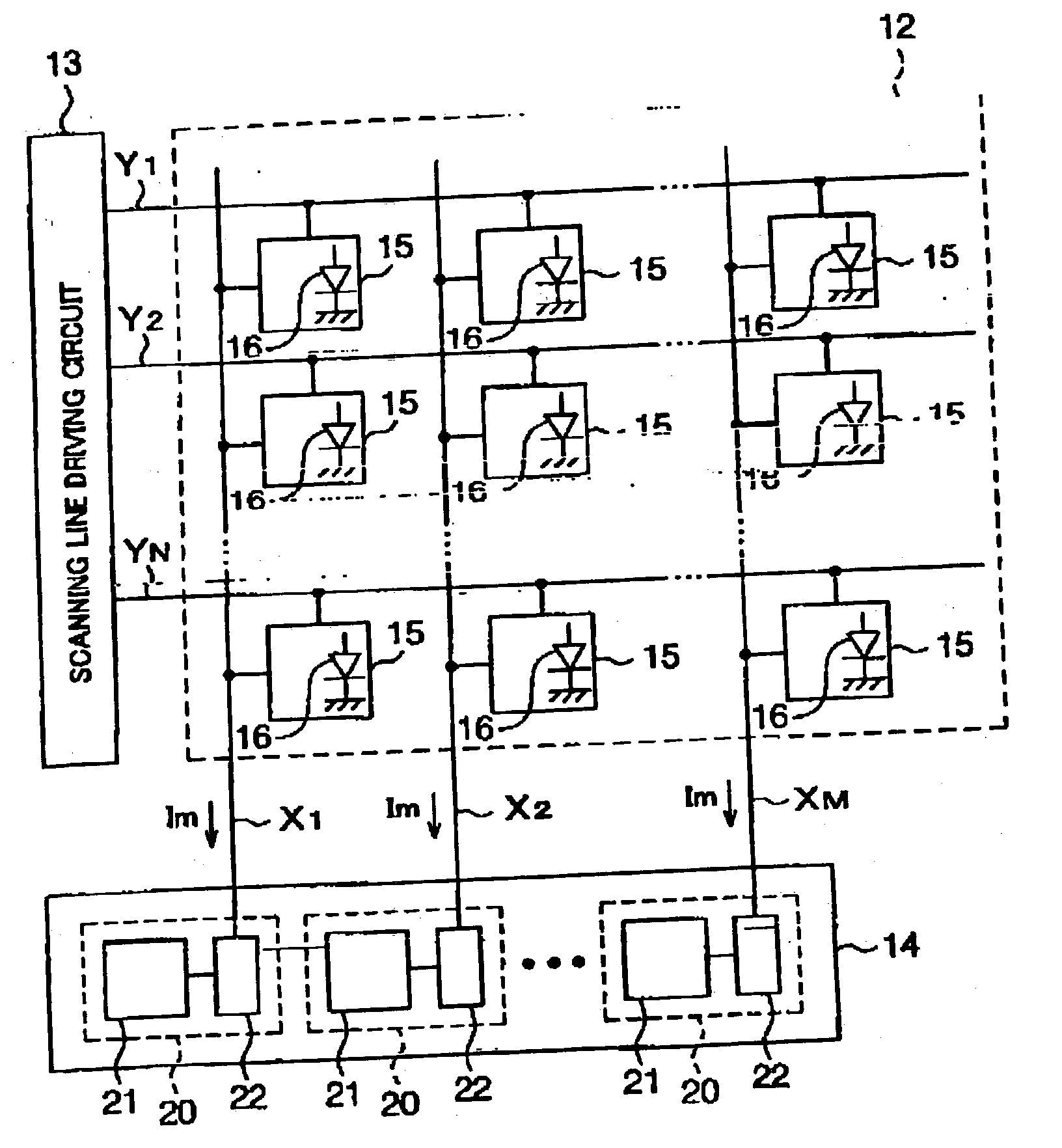
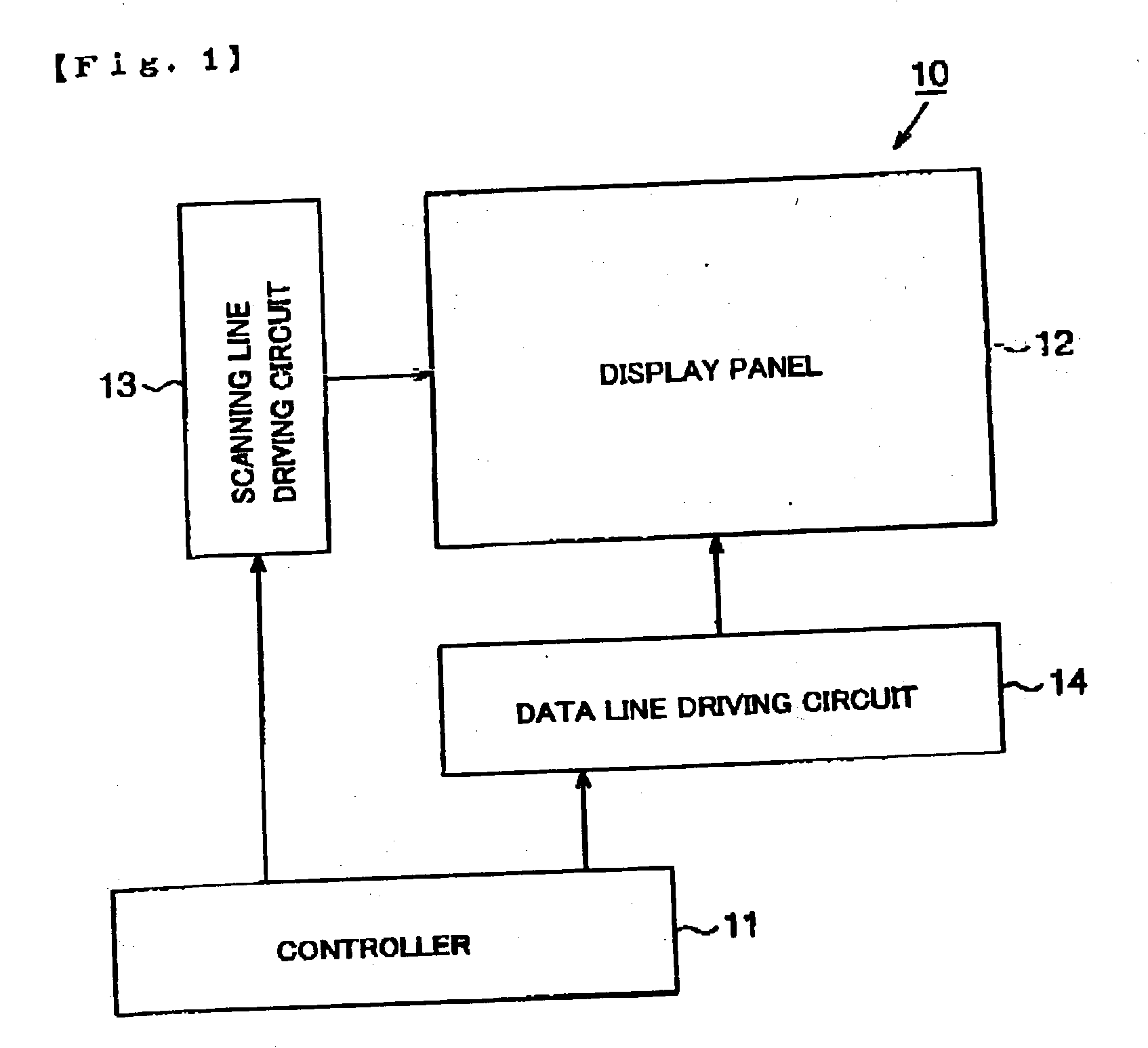
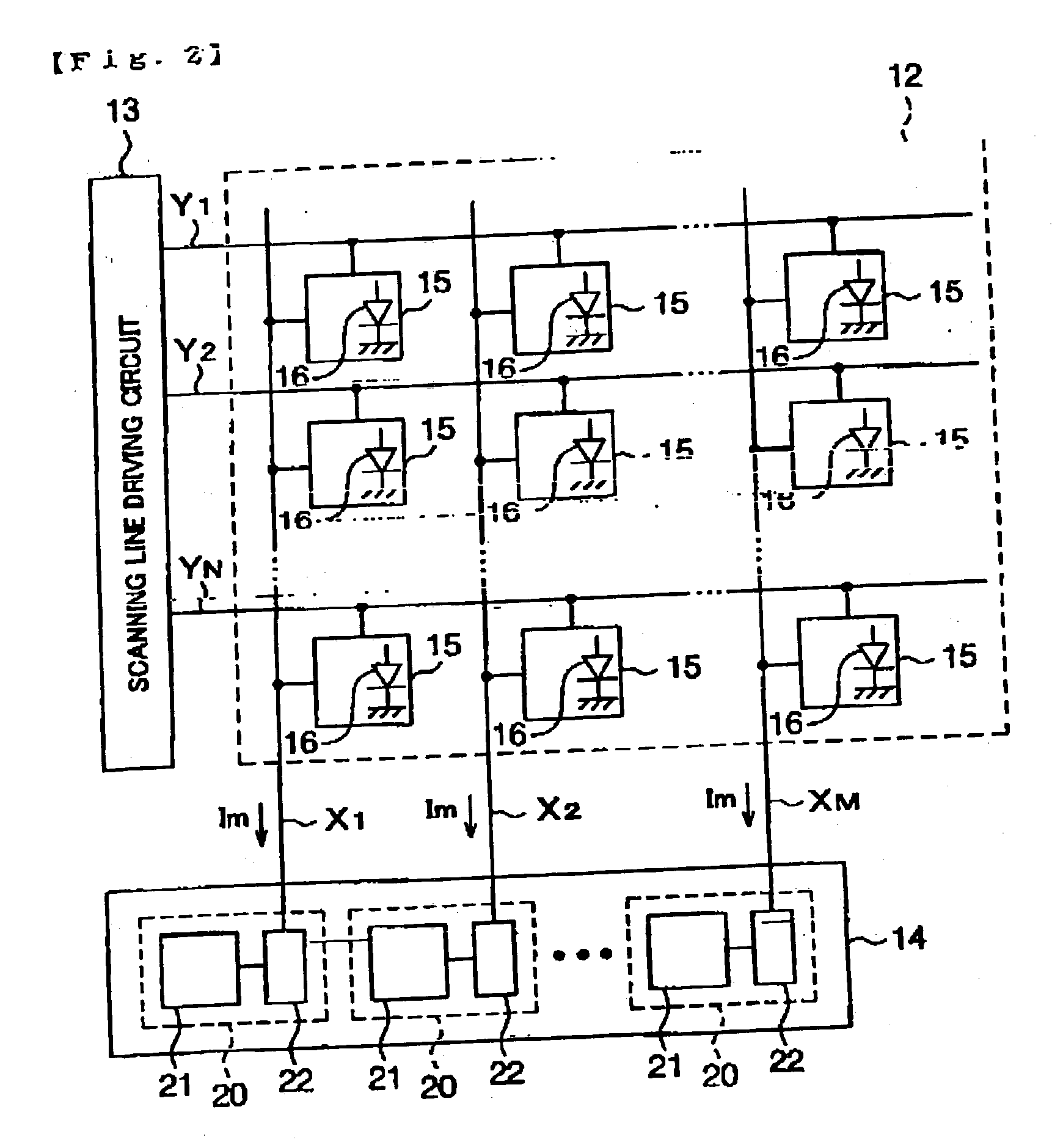
[0086] Hereinafter, a first embodiment specifying the present invention will be described with reference to FIGS. 1 to 4. FIG. 1 is a block circuit diagram illustrating a circuit structure of an active matrix type organic EL display of as an electro-optical device. FIG. 2 is a block circuit diagram illustrating an internal circuit structure of a display panel and data line driving circuit. FIG. 3 is a circuit diagram of a buffer circuit.

[0087] An organic EL display 10 includes a controller 11, a display panel 12, a scanning line driving circuit 13, and a data line driving circuit 14.

[0088] The controller 11, the scanning line driving circuit 13 and the data line driving circuit 14 of the organic EL display 10 may be formed of independent electronic parts, respectively. For example, each of the controller 11, the scanning line driving circuit 13 and the data line driving circuit 14 may be formed of a semiconductor integrated circuit device with one chip, resp...

second embodiment

[0140] [Second Embodiment]

[0141] An application of the organic EL display 10 as the electro-optical device explained in the first embodiment to an electronic apparatus will be described with reference to FIGS. 5 and 6. The organic EL display 10 can be applied to various electronic apparatuses such as a portable personal computer, a mobile phone, or a digital camera.

[0142] FIG. 6 is a perspective view illustrating a structure of a portable personal computer. In FIG. 6, a personal computer 50 includes a main body 52 with a keyboard 51 and a display unit 53 using the organic EL display 10.

[0143] In this case, the display unit 53 using the organic EL display 10 has the same effect as a display unit according to the above embodiment. As a result, it is possible to provide a portable personal computer 50 with a buffer circuit of a data line driving circuit that can be formed of a simpler circuit.

[0144] FIG. 7 is a perspective view illustrating a structure of a mobile phone. In FIG. 7, a m...


PUM


Abstract

[Object] To provide an electronic circuit, an electronic device and an electronic apparatus, which are capable of form a simple circuit. [Solving Means] A first buffer circuit 30 is formed of second, third and sixth transistors Tr2, Tr3 and Tr6 and a first capacitor C1. A second buffer circuit 40 is formed of fourth, fifth and seventh transistors Tr4, Tr5 and Tr7 and a second capacitor C2. The drain of the second transistor Tr2 of the first buffer circuit 30 and the drain of the fourth transistor Tr4 of the second buffer circuit 40 are connected to the first transistor Tr1. Furthermore, the drain of the sixth transistor Tr6 of the first buffer circuit 30 is connected to the drain of the seventh transistor Tr7 of the second buffer circuit 40 through an analog output terminal Po.

Description

[0001] 1. Field of Invention[0002] [Detailed Description of the Invention][0003] The present invention relates to an electronic circuit, an electronic device, and an electronic apparatus.[0004] 2. Description of Related Art[0005] [Description of the Related Art][0006] Recently, electro-optical devices using organic electro-luminescent (EL) elements have attracted attention. Because the organic EL elements are spontaneous emission elements, which do not need a back light, they are expected to realize display devices with low power consumption, large viewing angle, and high contrast ratio.[0007] The electro-optical device includes a data line driving circuit for supplying to each pixel circuit a data signal according to the luminance gradation of the organic EL element. The data line driving circuit is connected to a controller for outputting image data. The data line driving circuit includes a plurality of single-line drivers connected to each pixel circuit through data lines. Each s...

Claims


Application Information

Patent Timeline
Patent Type & Authority Applications(United States)
IPC IPC(8): H01L51/50G09G3/20G09G3/22G09G3/30G09G3/32
CPCG09G3/22G09G3/3216G09G3/325G09G2320/0223G09G2300/06G09G2300/0842G09G3/3275G09G3/30
Inventor KASAI, TOSHIYUKI
Owner ELEMENT CAPITAL COMMERCIAL CO PTE LTD
Why Eureka
Try Eureka