Microelectronic mechanical system and methods

a mechanical system and microelectronic technology, applied in the field of microelectronic mechanical system and methods, can solve the problems of performance degradation of the device, incompatibility of the typical method used to make mems and the method used to fabricate ics,

Inactive Publication Date: 2004-03-18
SILICON LIGHT MACHINES CORP
View PDF99 Cites 136 Cited by
  • Summary
  • Abstract
  • Description
  • Claims
  • Application Information

AI Technical Summary

Problems solved by technology

Unfortunately, typical methods for making MEMS are incompatible methods used to fabricate ICs.
Hence, MEMS and ICs are usually fabricated separately and laboriously combined in s

Method used


Image

  • Microelectronic mechanical system and methods
  • Microelectronic mechanical system and methods
  • Microelectronic mechanical system and methods

Examples


Embodiment Construction

:

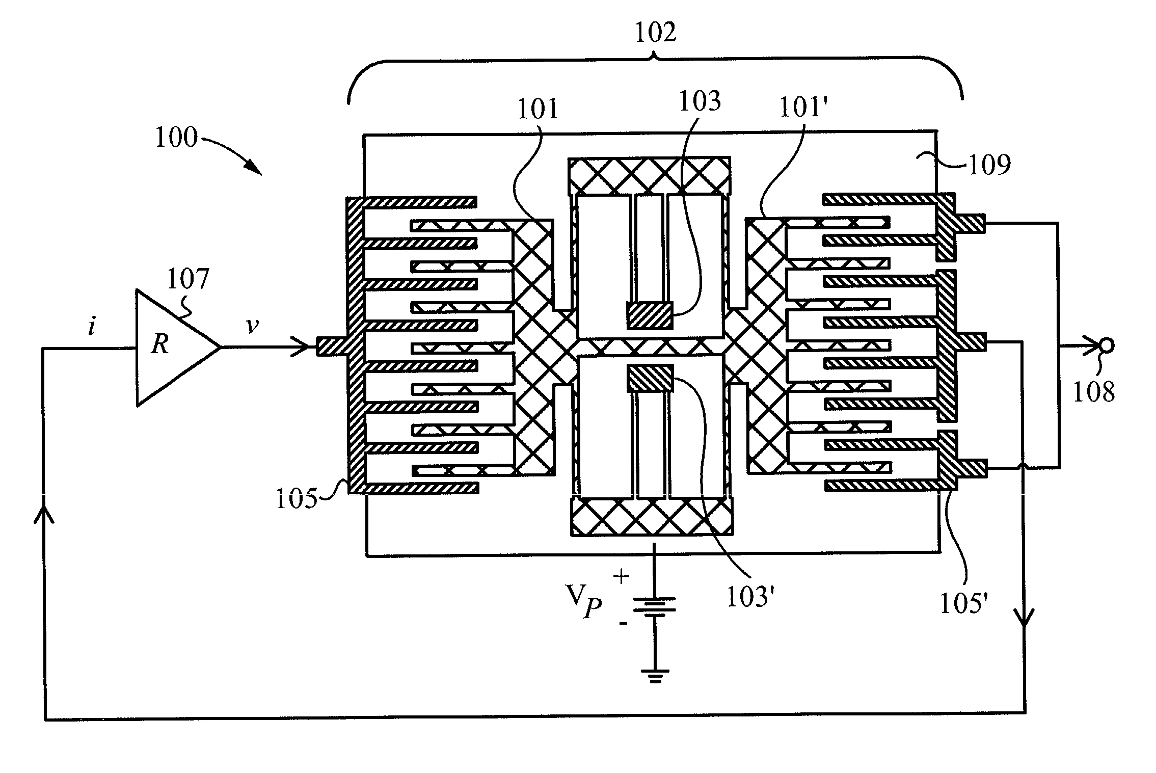
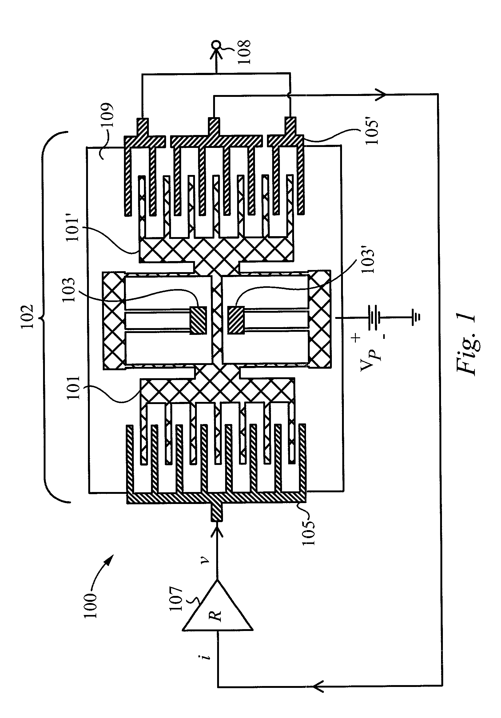
[0027] In general, the present invention provides a method to make devices with encapsulated release structures. The current invention is particularly useful for fabricating MEMS oscillators, optical display devices, optical transmission devices, RF devices and related devices. MEMS oscillators can have any number or simple or complex configurations, but they all operate on the basic principle of using the fundamental oscillation frequency of the structure to provide a timing signal to a coupled circuit. Referring to FIG. 1, a resonator structure 102 has a set of movable comb features 101 and 101' that vibrate between a set of matched transducer combs 105 and 105'. The resonator structure 102, like a pendulum, has a fundamental resonance frequency. The comb features 101 and 101' are secured to a ground plate 109 through anchor features 103 and 103'. In operation, a dc-bias is applied between the resonator 102 and a ground plate 109. An ac-excitation frequency is applied to the comb...


PUM

PropertyMeasurementUnit
Thicknessaaaaaaaaaa
Thicknessaaaaaaaaaa
Thicknessaaaaaaaaaa

Abstract

The current invention provides for encapsulated release structures, intermediates thereof and methods for their fabrication. The multi-layer structure has a capping layer, that preferably comprises silicon oxide and/or silicon nitride, and which is formed over an etch resistant substrate. A patterned device layer, preferably comprising silicon nitride, is embedded in a sacrificial material, preferably comprising polysilicon, and is disposed between the etch resistant substrate and the capping layer. Access trenches or holes are formed in to capping layer and the sacrificial material are selectively etched through the access trenches, such that portions of the device layer are release from sacrificial material. The etchant preferably comprises a noble gas fluoride NGF2x (wherein Ng=Xe, Kr or Ar: and where x=1, 2 or 3). After etching that sacrificial material, the access trenches are sealed to encapsulate released portions the device layer between the etch resistant substrate and the capping layer. The current invention is particularly useful for fabricating MEMS devices, multiple cavity devices and devices with multiple release features.

Description

[0001] The present invention relates to wafer processing. More particularly, the present invention relates to methods for encapsulation of microelectronic mechanical systems.BACKGROUND OF INVENTION[0002] The combination microelectronic mechanical systems (MEMS) and integrated circuits (ICs) allows for the possibility to make any number of micro-sensors, transducers and actuators. Unfortunately, typical methods for making MEMS are incompatible methods used to fabricate ICs. Hence, MEMS and ICs are usually fabricated separately and laboriously combined in subsequent and separate steps.[0003] In addition to the MEMS and ICs processing incompatibilities, MEMS typically require encapsulation, whereby the active portions of the MEMS are sealed within a controlled storage environment. One way to encapsulate the active portions of the MEMS is to provide unique customized packaging structure configured with conductive leads fitted for the MEMS. Alternatively, the MEMS can be formed on a wafe...

Claims


Application Information

Patent Timeline
IPC IPC(8): B81B3/00B81C1/00B81B7/00H01L21/46H02N1/00H03H9/24
CPCB81B2201/0271B81B2203/0136B81C1/00246B81C1/00333B81C2203/0735B81C2201/0109B81C2201/014B81C2203/0136B81C1/00484
Inventor BRUNER, MIKE
Owner SILICON LIGHT MACHINES CORP
Why Eureka
Try Eureka