Spin valve transistor with stabilization and method for producing the same

a technology of spin valve transistor and stabilization, which is applied in the field of spin valve transistor with stabilization and the production of the same, can solve the problems of reducing the signal-to-noise ratio, rising to an irreproducible response of the head, and difficulty in maintaining a single magnetic domain sta

Inactive Publication Date: 2004-06-03
HITACHI GLOBAL STORAGE TECH NETHERLANDS BV
View PDF6 Cites 22 Cited by
  • Summary
  • Abstract
  • Description
  • Claims
  • Application Information

AI Technical Summary

Problems solved by technology

One of the problems with such a MR read head, however, lies in developing a structure that generates an output signal that is both stable and linear with the magnetic field strength from the recorded medium.
If some means is not used to maintain the ferromagnetic sensing layer of the SVT device (i.e., the ferromagnetic layer whose moment is not fixed) in a single magnetic domain state, the domain walls of magnetic domains will shift positions within the ferromagnetic sensing layer, causing noise which reduces the signal-to-noise ratio and which may give rise to an irreproducible response of the head.
The problem of maintaining a single magnetic domain state is especially difficult in the case of an SVT MR read head because, unlike an AMR sensor, the sense current passes perpendicularly through the ferromagnetic layers and the tunnel barrier layer, and thus any metallic materials in direct contact with the edges of the ferromagnetic layers will short circuit the electrical resistance of the read head.
The drawbacks of some of the conventional devices are that the magnetic state of the device during non-operation, or during the non-active state, is not known.
This causes the free layer to "wander", wherein the magnetization of the free layer is not oriented in a proper position resulting in an unstable device.

Method used


Image

  • Spin valve transistor with stabilization and method for producing the same
  • Spin valve transistor with stabilization and method for producing the same
  • Spin valve transistor with stabilization and method for producing the same

Examples


Embodiment Construction

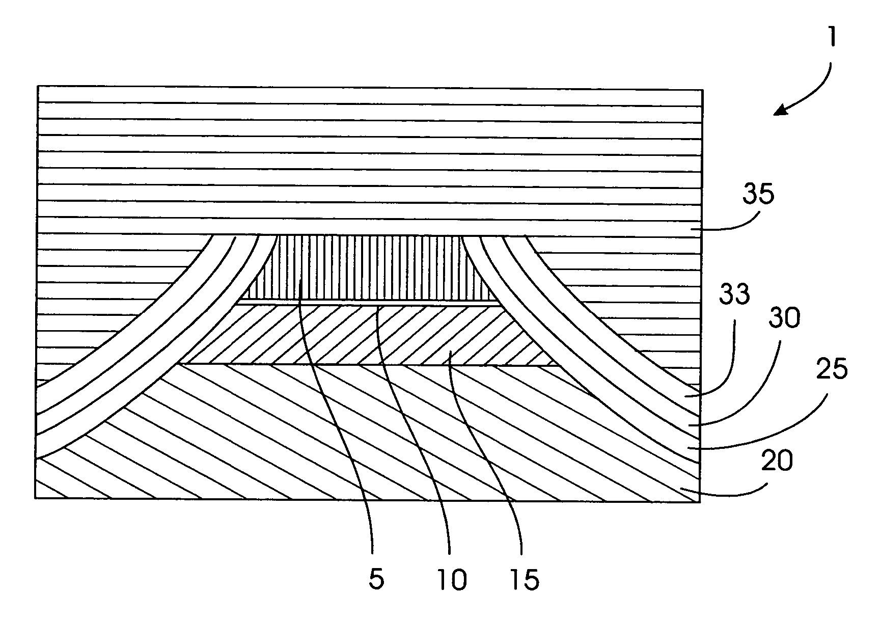
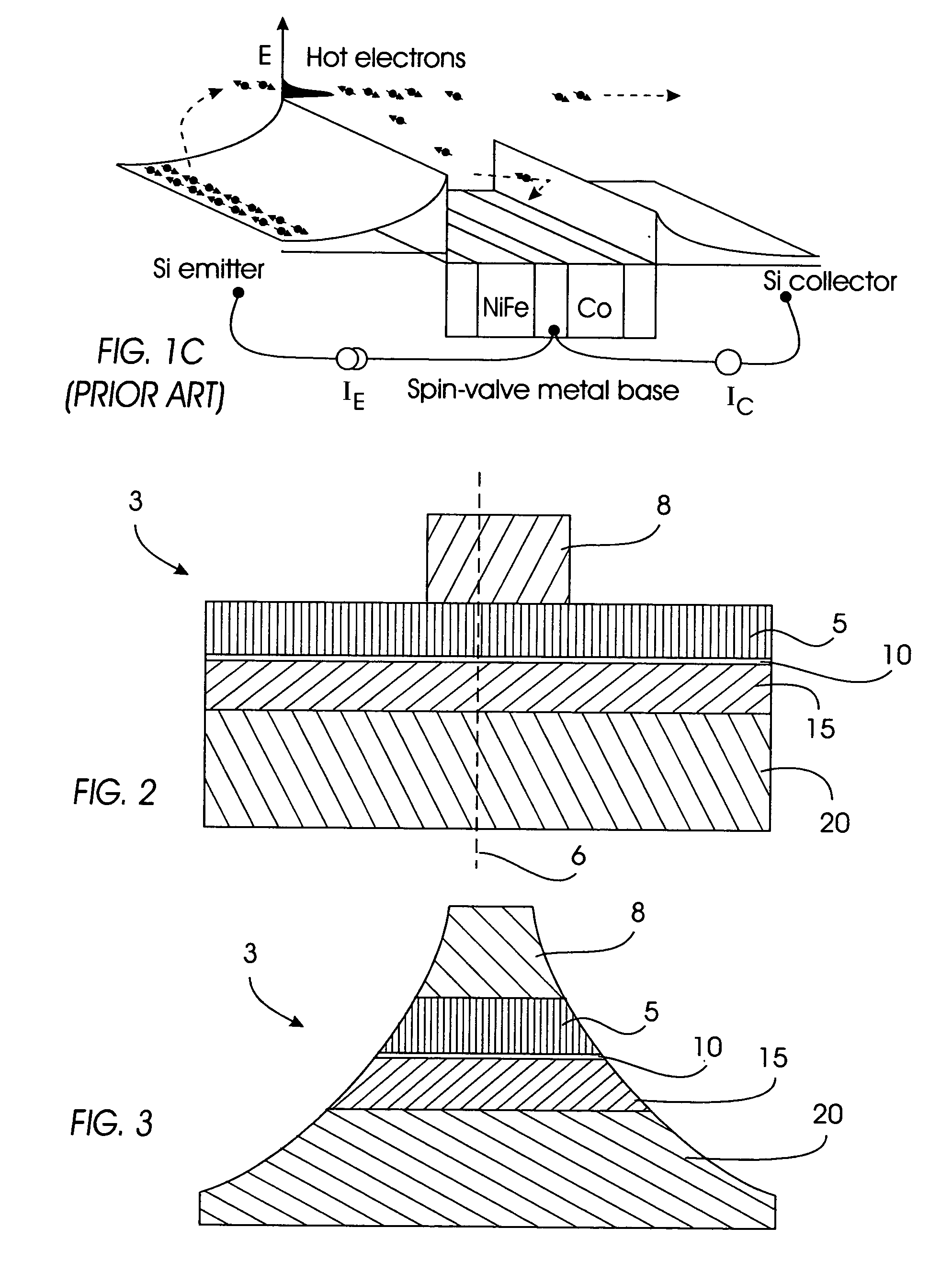
[0053] As previously mentioned, there is a need for a novel spin valve transistor device having insulating hard bias stabilization. Referring now to the drawings, and more particularly to FIGS. 2 through 20(b), there are shown preferred embodiments of the method and structures according to the present invention, in which there is provided a spin valve transistor 1 comprising a magnetic field sensor 3, an insulating layer 25 adjacent to the magnetic field sensor 3, and a hard bias layer 30 adjacent to the insulating layer 25.

[0054] The processing steps involved in manufacturing the SVT 1 are sequentially illustrated in FIGS. 2 through 8, and in FIGS. 9 through 20(b), wherein there is shown in FIG. 2 a magnetic field sensor 3 comprising a base region 15, a collector region 20 adjacent the base region 15, an emitter region 5 adjacent the base region 15, and a barrier region 10 located between the base region 15 and the emitter region 5. A resist layer 8 is further shown adjacent the me...


PUM

PropertyMeasurementUnit
thicknessaaaaaaaaaa
thicknessaaaaaaaaaa
thicknessaaaaaaaaaa

Abstract

A method and structure for a spin valve transistor (SVT) comprises a magnetic field sensor, an insulating layer adjacent the magnetic field sensor, a bias layer adjacent the insulating layer, a non-magnetic layer adjacent the bias layer, and a ferromagnetic layer over the non-magnetic layer, wherein the insulating layer and the non-magnetic layer comprise antiferromagnetic materials. The magnetic field sensor comprises a base region, a collector region adjacent the base region, an emitter region adjacent the base region, and a barrier region located between the base region and the emitter region. The bias layer is between the insulating layer and the non-magnetic layer. The bias layer is magnetic and is at least three times the thickness of the magnetic materials in the base region.

Description

[0001] This application is a continuation-in-part of U.S. patent application Ser. No. 10 / 307,062, filed Nov. 29, 2002, entitled "Spin Valve Transistor With Stabilization and Method for Producing the Same", the complete disclosure of which is herein incorporated by reference.[0002] 1. Field of the Invention[0003] The present invention generally relates to magnetoelectronic devices, and more particularly to a spin valve transistor (SVT) having an insulating hard bias stabilization.[0004] 2. Description of the Related Art[0005] A spin valve transistor is a vertical spin injection device which has spin oriented electrons injected over a barrier into a free layer, and is used as a magnetic field sensor device. Those spin oriented electrons that are not spin scattered continue and then traverse a second barrier. The current over the second barrier is referred to as the magneto-current. Conventional devices are constructed using silicon wafer bonding to define the barriers.[0006] Conventio...

Claims


Application Information

Patent Timeline
Patent Type & Authority Applications(United States)
IPC IPC(8): G11B5/00G11B5/39H01F10/32H01F41/30H01L29/66
CPCB82Y10/00B82Y25/00B82Y40/00G11B5/3906G11B5/3932G11B2005/0008Y10T29/49039H01F10/3268H01F41/302H01L29/66984H01F41/325Y10T29/49043Y10T29/49044G11B2005/3996
Inventor FONTANA, ROBERT E. JR.LILLE, JEFFREY S.
Owner HITACHI GLOBAL STORAGE TECH NETHERLANDS BV
Why Eureka
Try Eureka