

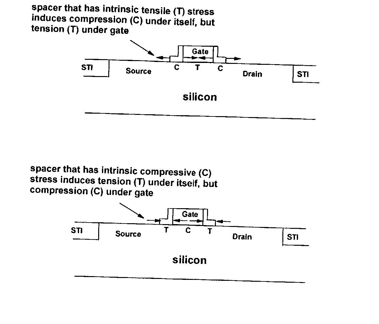
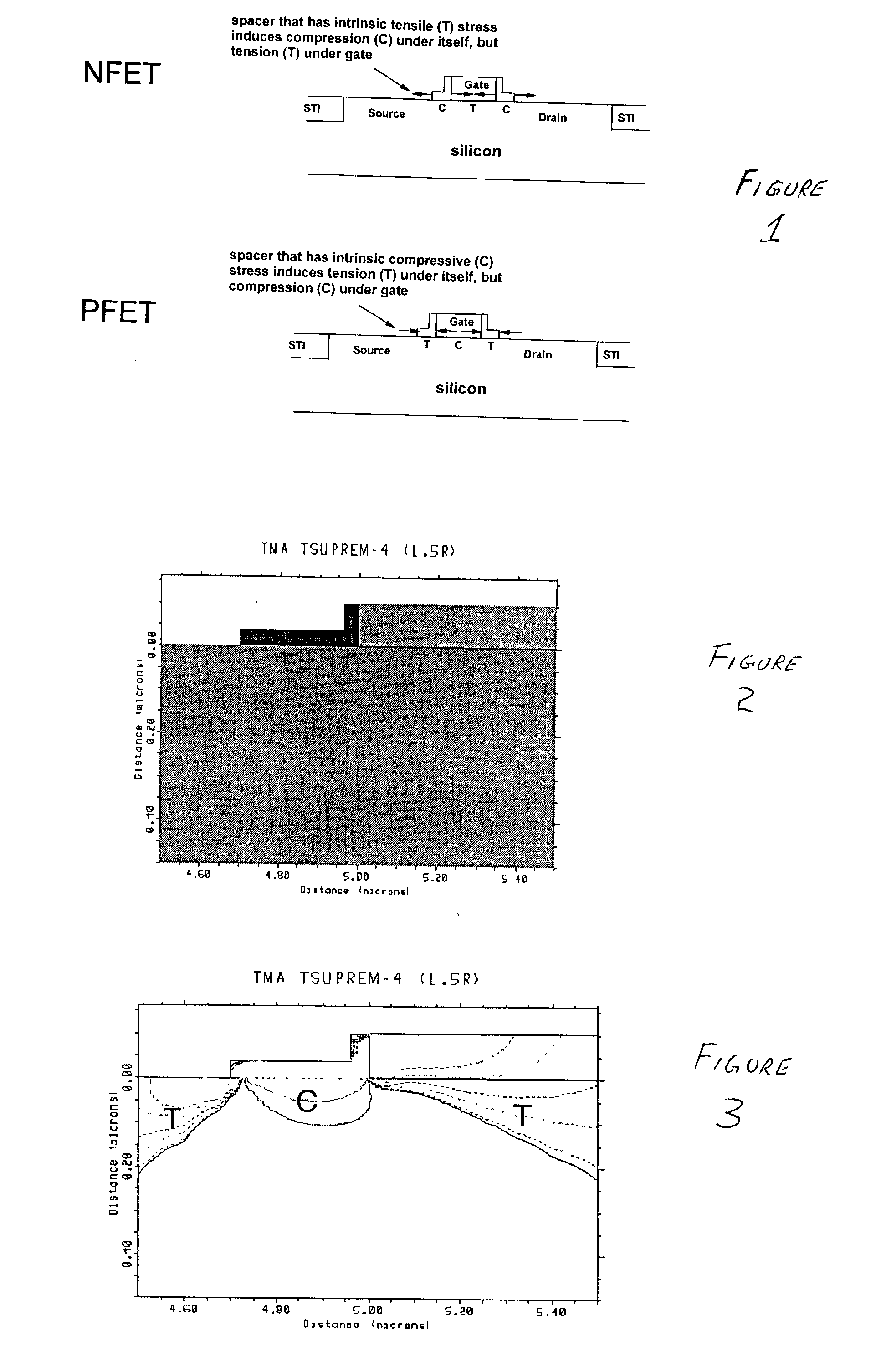
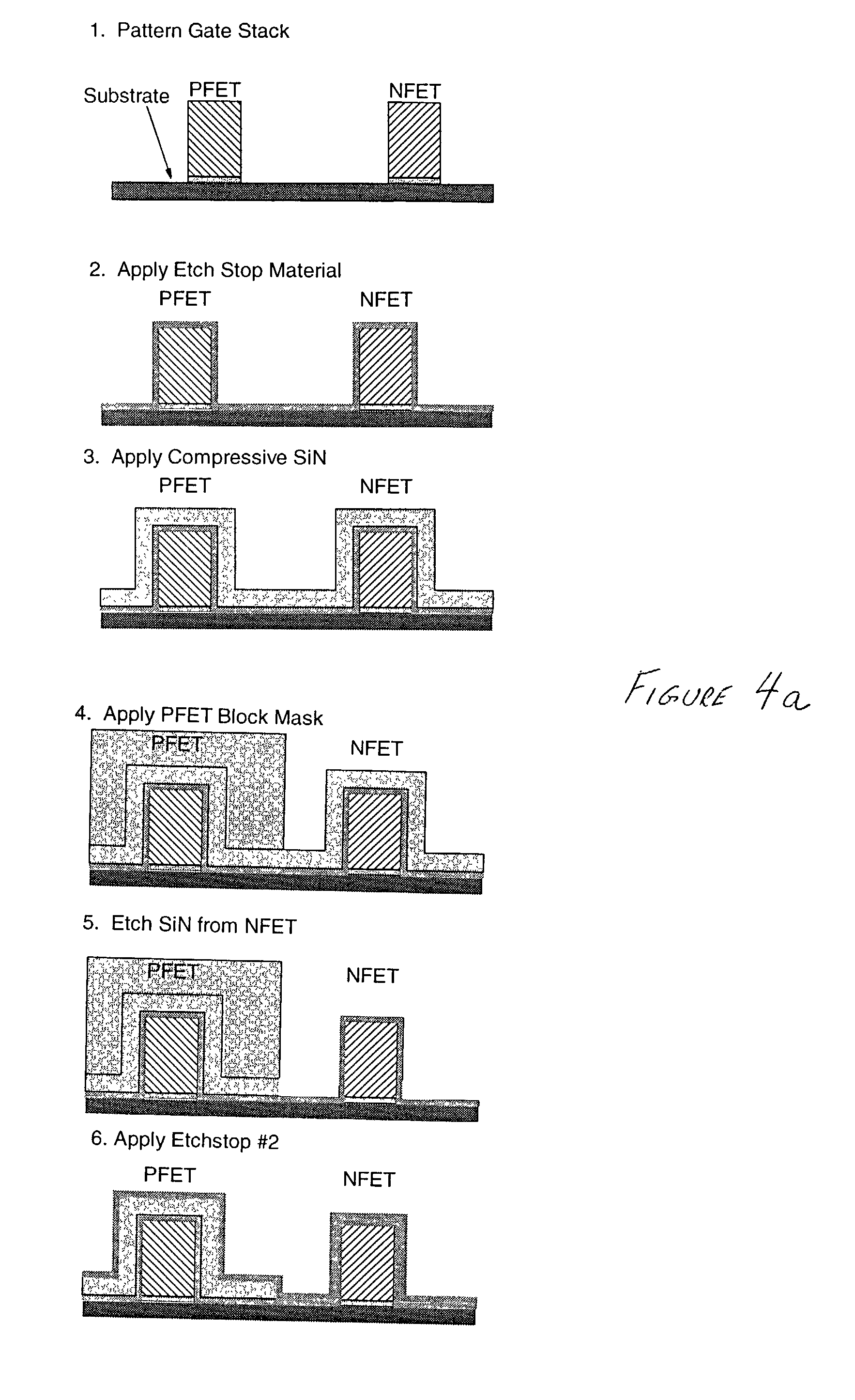
Stress inducing spacers
a stress inducing spacer and spacer technology, applied in the direction of electrical transducers, semiconductor devices, transducer details, etc., can solve the problems of centered compressive stress in the channel, and the inability to improve the performance of both pfet and nfet simultaneously
- Summary
- Abstract
- Description
- Claims
- Application Information
AI Technical Summary
Benefits of technology
Problems solved by technology
Method used
Image

Examples
Embodiment Construction
[0038] It will be appreciated that, although specific embodiments of the invention have been described herein for purposes of illustration, various modifications may be made without departing from the spirit and scope of the invention. In particular, while nitride is a good material choice for the two spacers because the intrinsic stress can be controlled from tension to compression. While this above embodiment with nitride spacers is preferred, this approach is not restricted in material choice. One can have additional options in terms of the material set. HDP can be used for compressive stress while TEOS can be used for tension. The integration of these material choices causes changes in process flow.
[0039] Other spacer materials can be used, such as ceramics and silicon carbide, which can also impart intrinsic stresses. The general view of stresses in silicon is that it's disadvantageous. Stresses lead to ruptures or dislocations in the lattice structure, which lead to junction l...
PUM
 Abstract
Description
Claims
Application Information