Photoresist composition
a technology of composition and photoresist, applied in the field of photoresist composition, can solve the problems of poor adhesive property to silicon substrate, degradation of photoresist film development, and inconvenient use of photoresist resins for vuv photoresist films
- Summary
- Abstract
- Description
- Claims
- Application Information
AI Technical Summary
Benefits of technology
Problems solved by technology
Method used
Image
Examples
example 1
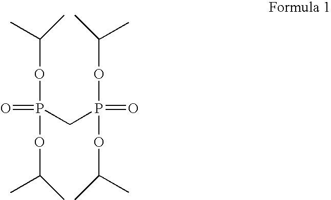
[0028] Variation of light absorbance depending on the added amount of TIMD (1)
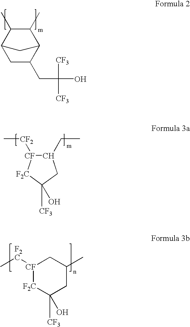
[0029] Poly(norbomenehexafluoroalcohol) of the above Formula 2 which is photoresist polymer for 157 nm was mixed with TIMD as an addtive in an amount ranging from 0 to 20 wt %. Then, the resultant was coated on a substrate at a thickness of 2000 .ANG. to form a thin photoresist film.
[0030] Next, the light absorbance of the thin film measured using an ellipsometer of Sematech was shown in Table 1 and FIG. 1. The light absorbance was obtained by calculating light absorbance to the thin film having a thickness of 2000 .ANG. in terms of a value to the thickness of 1 .mu.m. The value of .alpha.10 to a light source of 157.6 nm was shown in FIG. 1.
1TABLE 1 Amount of added n k .alpha.(.mu.m.sup.-1) .alpha..sub.10 .alpha.(.mu.m.sup.-1) .alpha..sub.10 TIMD (%) (157.6 nm) (157.6 nm) (157.6 nm) (157.6 nm) (193 nm) (193 nm) 0 1.667 0.049 3.87 1.68 0.25 0.107 5 1.667 0.046 3.70 1.61 -- --10 1.687 0.045 3.56 1.55 0.19 0...
example 2
[0031] Variation of light absorbance depending on the amount of added TIMD (2)
[0032] The blend polymer of Formula 3a and 3b which is photoresist polymer for 157 nm were mixed with TIMD as an addtive in an amount ranging from 0 to 20 wt %. Then, the resultant was coated on a substrate at a thickness of 2000 .ANG. to form a thin photoresist film.
[0033] Next, the light absorbance of the thin film measured using an ellipsometer of Sematech was shown in Table 2 and FIG. 2. The light absorbance was obtained by calculating light absorbance to the thin film having a thickness of 2000 .ANG. in terms of a value to the thickness of 1 .mu.m. The value of .alpha.10 to a light source of 157.6 nm was shown in FIG. 2.
2TABLE 2 Amount of added .alpha.(.mu.m.sup.-1) .alpha..sub.10 .alpha.(.mu.m.sup.-1) .alpha..sub.10 TIMD (%) n (157.6 nm) k (157.6 nm) (157.6 nm) (157.6 nm) (193 nm) (193 nm) 0 1.553 0.019 1.52 0.66 0.32 0.139 5 1.580 0.012 0.99 0.43 -- --10 1.573 0.013 0.99 0.43 0.23 0.098 15 1.591 0....
PUM
| Property | Measurement | Unit |
|---|---|---|
| wavelength | aaaaa | aaaaa |
| wavelength | aaaaa | aaaaa |
| wavelength | aaaaa | aaaaa |
Abstract
Description
Claims
Application Information


