Chip design verifying and chip testing apparatus and method

Inactive Publication Date: 2004-07-15
PARK HYUNJU +1
View PDF8 Cites 32 Cited by
  • Summary
  • Abstract
  • Description
  • Claims
  • Application Information

AI Technical Summary

Problems solved by technology

In embodying a large-sized and complicated circuit on the ASIC element, one of the most troublesome cores relates to a verification of a proper operation of the designed circuit during a simulation and a system operation.
This is one of the greatest causes of the ASIC failure occurred when a simulation is sufficiently not performed.
As a circuit to be designed becomes complicated, and an intellectual property (IP) blocks to be recycled becomes increased in number, it becomes more difficult to make out a pattern of a simulation that can perfectly perform an operation of a chip on a system.
Particularly, in case of a circuit having millions of gates, it requires much time to perform a simulation that is operated by a command language of a microprocessor.
Therefore, since it does not use a data compression method for a data transmission between a main memory of and a hardware board of a computer, a performance improvement is limited.
In addition, as a hardware configuration of a circuit becomes complicated, a large number of hardware boards should be provided.
Moreover, the

Method used


Image

  • Chip design verifying and chip testing apparatus and method
  • Chip design verifying and chip testing apparatus and method
  • Chip design verifying and chip testing apparatus and method

Examples


Embodiment Construction

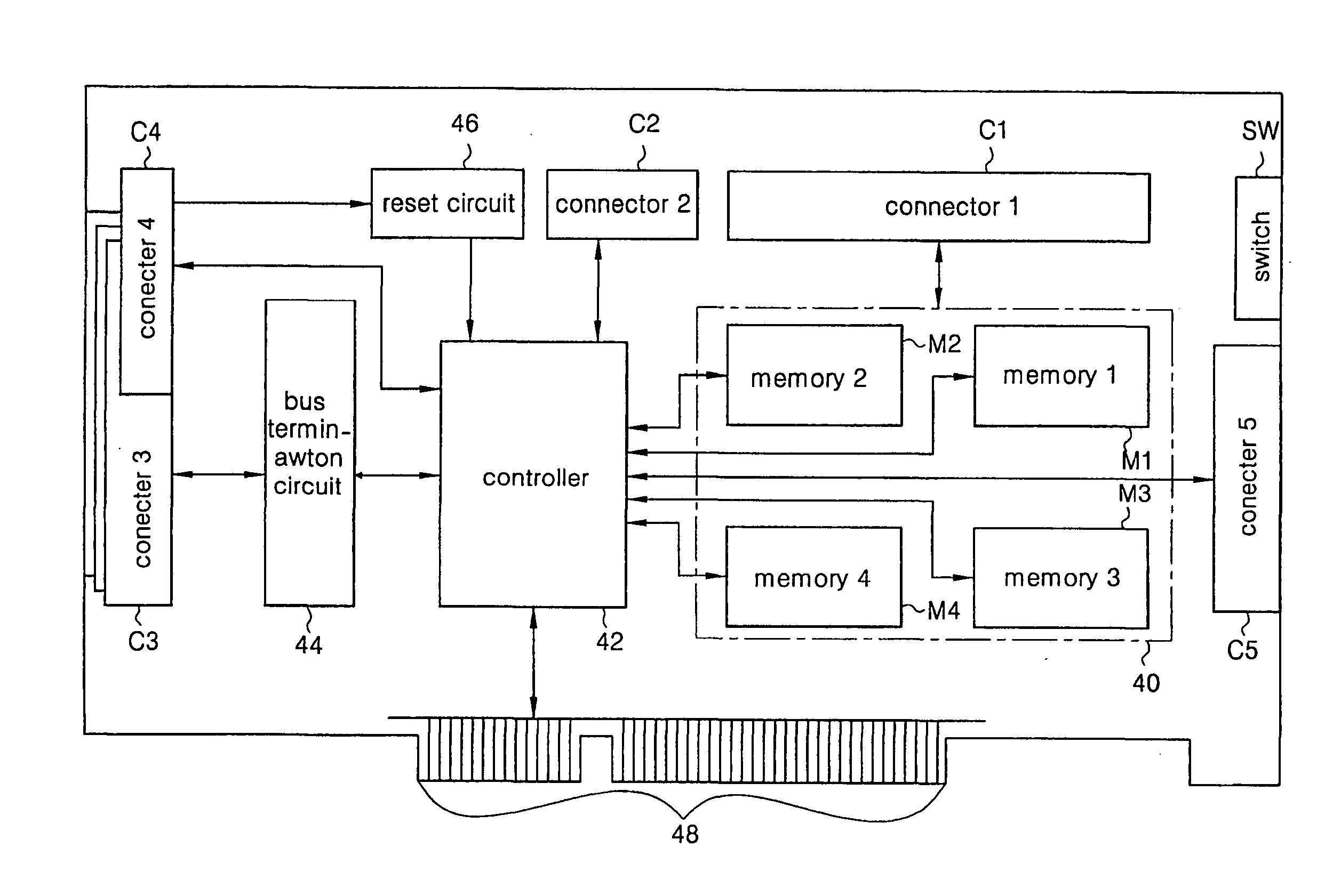
[0044] Reference will now be made in detail to a preferred embodiment of the present invention, example of which is illustrated in the accompanying drawings.

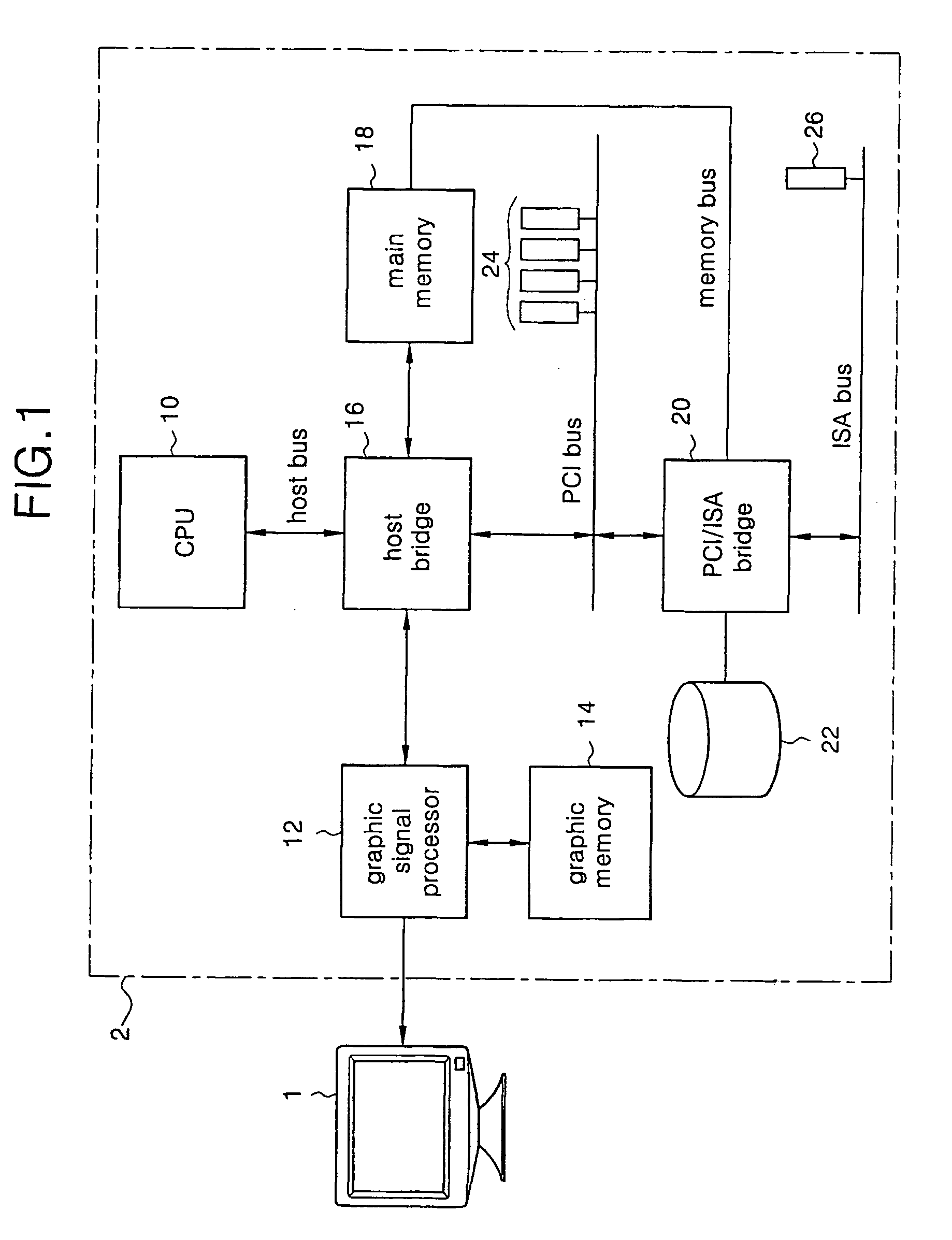
[0045] Returning now to FIG. 1, which shows a configuration of a typical computer system, the computer system includes a monitor 1 and a computer mainframe 2. The computer mainframe 2 includes a central processing unit (CPU) 10, a graphic signal processor 12, a graphic memory 14, a host bridge 16, a main memory 18, a PCI / ISA bridge 20, a hard disk drive 22, PCI slots 24, and an ISA slot 26.

[0046] The CPU 10 executes an application program and performs a function to control the computer system. The host bridge 16 performs an interface function among the CPU 10, the main memory 18, the graphic signal processor 12, the PCI / ISA bridge 20, and the PCI slots 24. The main memory 18 stores application programs and various kinds of input / output data that the CPU 10 brings from the hard disk 22. The graphic signal processor 12 is connecte...


PUM


Abstract

A chip design verifying and chip testing apparatus includes a storing means for storing an application program verifying an operation of a designed chip and testing a manufactured chip having a plurality of blocks, an I/O file, and a test vector; an interface means controlling a data transmission between the storing means and the chip, and having a data applying means for applying the I/O file and/or the test vector outputted from the storing means and a data storing means for storing data outputted from the chip; and a computer including a CPU for performing and controlling the application program.

Description

CROSS REFERENCE[0001] This application claims the benefit of Korean Patent Application No. 2000-30625, filed on Jun. 3, 2000 and the benefit of Korean Patent Application No. 2000-42575, filed on Jul. 25, 2000, under 35 U.S.C. .sctn. 119, the entirety of which are hereby incorporated by reference.[0002] 1. Field of the Invention[0003] The present invention relates to a chip design verifying and chip testing apparatus and method.[0004] 2. Description of Related Art[0005] As electronic design automation (EDA) tools, which relates to a design automation and a design technique utilizing a hardware description language (HDL), are widely used in various electronic industrial fields, a design circumstance of an application specific integrated circuit (ASIC) has become greatly improved. For example, compared with the existing circuits having a capacity of from tens of thousands to hundreds of thousands of gates, recently circuits have been designed to have a capacity of millions of gates, an...

Claims


Application Information

Patent Timeline
IPC IPC(8): G01R31/3183G01R31/3187G01R31/319G06F11/26G06F17/50
CPCG01R31/318357G06F17/5022G06F11/261G01R31/3187G06F30/33
Inventor PARK, HYUN JUYUN, DONG GOO
Owner PARK HYUNJU
Why Eureka
Try Eureka