Apparatus for fabricating semiconductor devices, heating arrangement, shower head arrangement, method of reducing thermal disturbance during fabrication of a semiconductor device, and method of exchanging heat during fabrication of a semiconductor device

a technology of semiconductor devices and shower heads, which is applied in the direction of coatings, chemical vapor deposition coatings, metallic material coating processes, etc., can solve the problems of equipment damage, thermal disturbance, and worker safety threats,

Inactive Publication Date: 2004-08-26
SAMSUNG ELECTRONICS CO LTD
View PDF19 Cites 23 Cited by
  • Summary
  • Abstract
  • Description
  • Claims
  • Application Information

AI Technical Summary

Benefits of technology

[0011] In another exemplary embodiment, the first heat part is disposed between the outer wall of the process chamber and the susceptor, and surrounds a circumference of the susceptor in a coiled shape. In another exemplary embodiment, a liner is disposed between the first heat part of the heat pipe and the susceptor to reduce the likelihood or prevent a process byproduct from being attached to the first supply pipe. According to an exemplary embodiment, the third heat part extends from the first heat part and surrounds the circumference of the shower part in a coiled shape.
[0018] In another exemplary embodiment, a method of reducing thermal disturbance during fabrication of a semiconductor device includes heating a first source gas to be supplied to a process chamber above room temperature and heating all other source gases to be supplied to the process chamber above room temperature.

Problems solved by technology

However, the conventional MOCVD apparatus may have the following drawbacks.
Additionally, equipment may be damaged and worker's safety may be threatened since the outer wall of the process chamber 120 is heated at a high temperature.
Further, a thermal disturbance may be generated and the reaction may be deteriorated due to a temperature difference between the first and second source gases, since the first source gas is supplied to the showerhead 140 in a heated state while the second source gas is supplied to the showerhead 140 at room temperature.

Method used


Image

  • Apparatus for fabricating semiconductor devices, heating arrangement, shower head arrangement, method of reducing thermal disturbance during fabrication of a semiconductor device, and method of exchanging heat during fabrication of a semiconductor device
  • Apparatus for fabricating semiconductor devices, heating arrangement, shower head arrangement, method of reducing thermal disturbance during fabrication of a semiconductor device, and method of exchanging heat during fabrication of a semiconductor device
  • Apparatus for fabricating semiconductor devices, heating arrangement, shower head arrangement, method of reducing thermal disturbance during fabrication of a semiconductor device, and method of exchanging heat during fabrication of a semiconductor device

Examples


Embodiment Construction

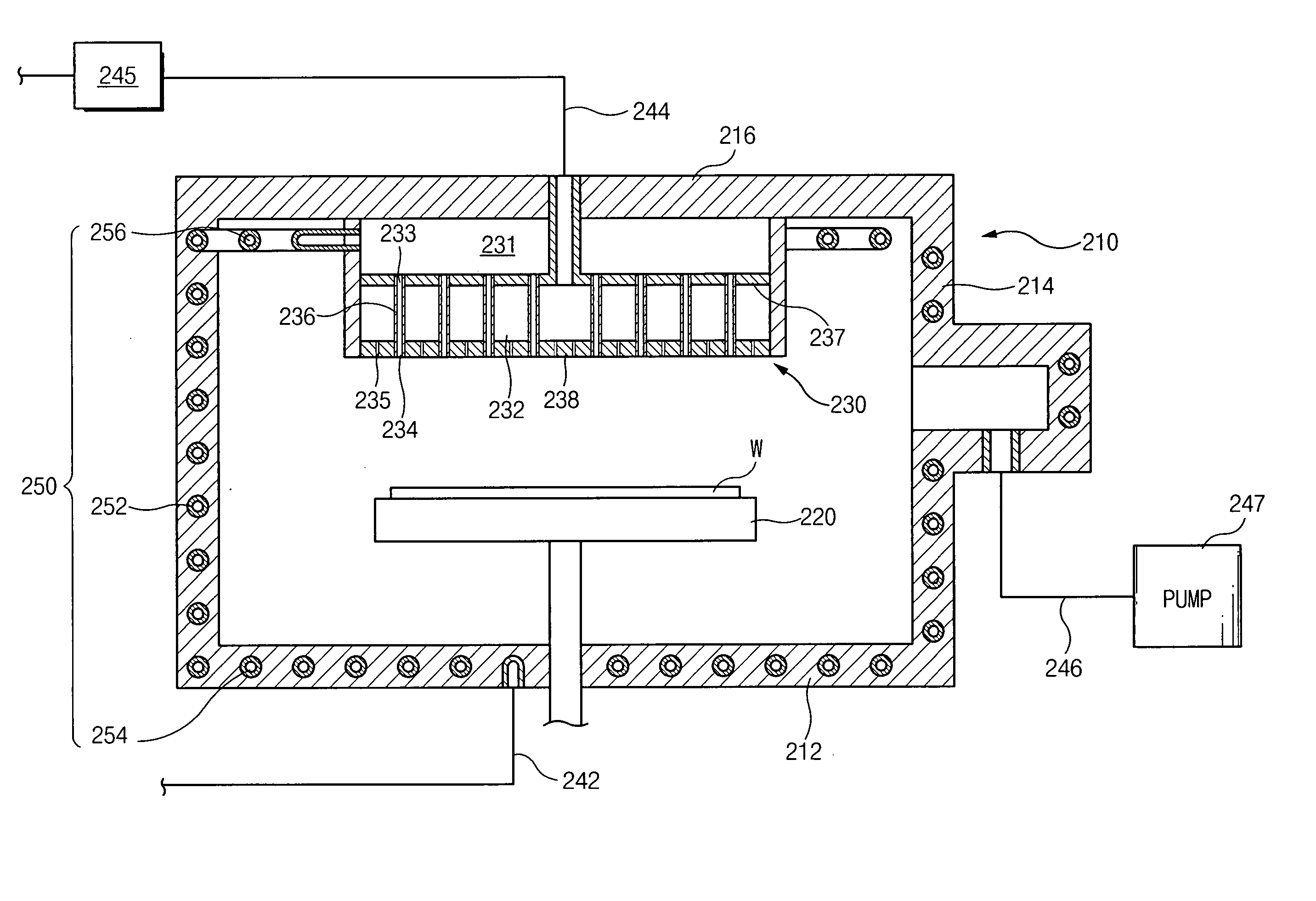
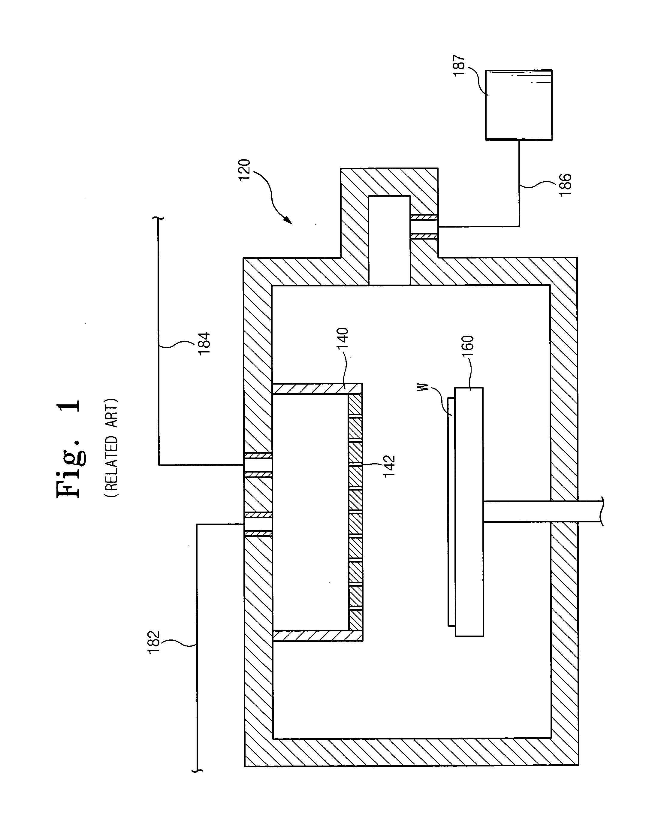
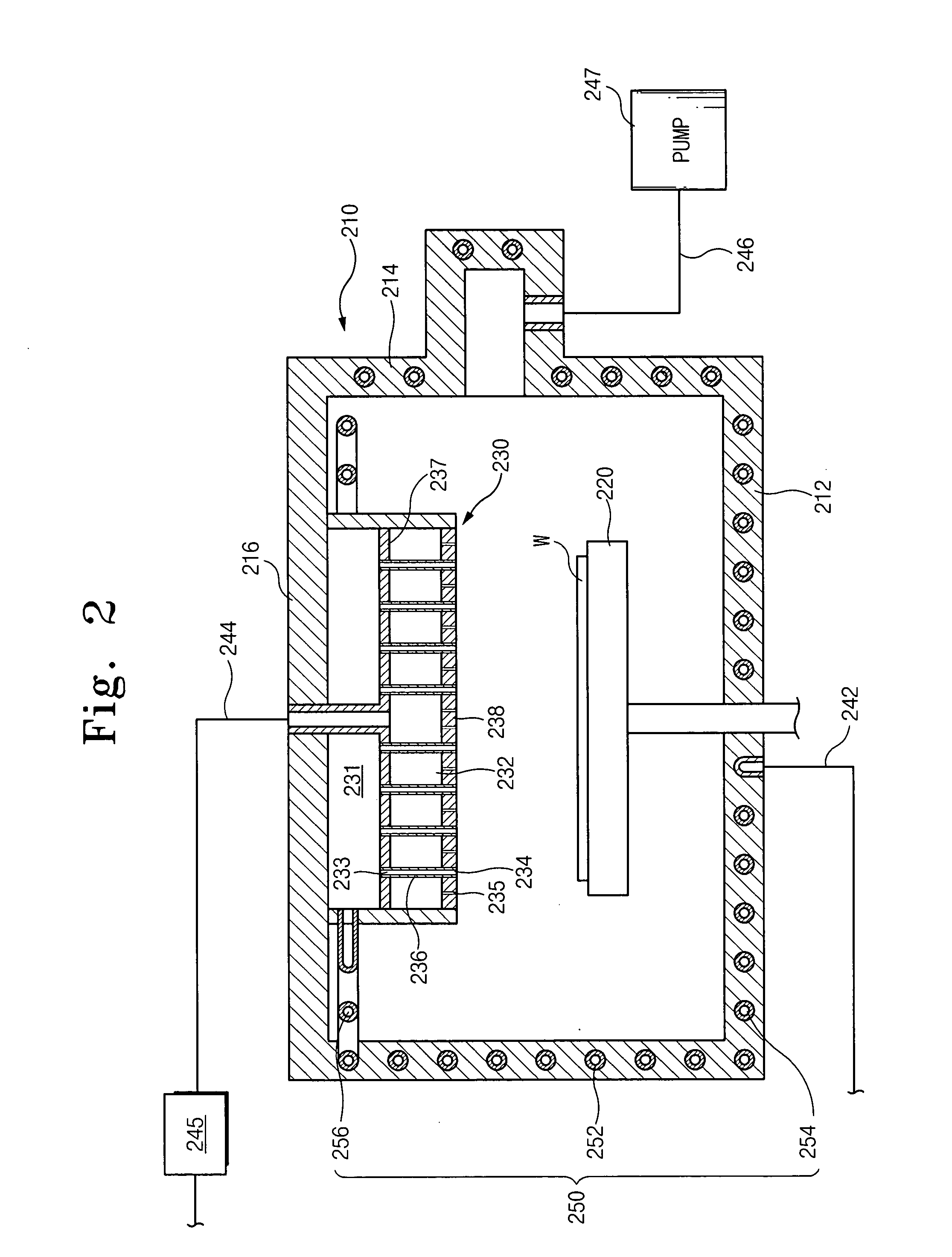
[0030] Reference will now be made in detail to the exemplary embodiments of the present invention, which are illustrated in the accompanying drawings. It should be recognized that the present invention is not limited by any of the details of the exemplary embodiments explained herein, but embodied in different forms. The exemplary embodiments of the present invention are provided merely to thoroughly completely convey ideas of the present invention to those skilled in the art that the present invention pertains to.

[0031] In the following exemplary embodiments, a metal organic chemical vapor deposition (MOCVD) apparatus is exemplified for description, but the apparatus of the present invention may be used in any other type of apparatus for fabricating a semiconductor device in which a film is formed on a wafer at higher than room temperature.

[0032] Further, the inventive apparatus may be used in a deposition method for simultaneously supplying source gases into a process chamber (suc...


PUM

PropertyMeasurementUnit
temperatureaaaaaaaaaa
circumferenceaaaaaaaaaa

Abstract

An apparatus for fabricating a semiconductor device in which a substance is deposited on a semiconductor wafer. The apparatus includes a heating arrangement and / or a shower head arrangement. The shower head arrangement supplies at least two source gases to the apparatus. The heating arrangement heats at least one of the source gases supplied to a process chamber of the apparatus. The heating arrangement may include a heat pipe including at least one part. A method of reducing thermal disturbance during fabrication of a semiconductor device using the heating arrangement and a method of exchanging heat during fabrication of the semiconductor device using the heating arrangement.

Description

[0001] The application claims the benefit of the priority of Korean Patent Application No. 2003-11778, filed on Feb. 25, 2003 and Korean Patent Application No. 2003-51434, filed on Jul. 25, 2003, in the Korean Intellectual Property Office, the entire contents of both of which are hereby incorporated by reference.[0002] The present invention relates to an apparatus for fabricating a semiconductor device, a heating arrangement, a shower head arrangement, a method of reducing thermal disturbance during fabrication of a semiconductor device, and a method of exchanging heat during fabrication of a semiconductor device.DESCRIPTION OF THE RELATED ART[0003] Several processes, such as an ion implanting process, a deposition process, a photolithography process and an etching process may be used to fabricate semiconductor devices. Among these processes, the deposition process is used for forming a film on a wafer and may be further classified into a chemical vapor deposition method and a physi...

Claims


Application Information

Patent Timeline
Patent Type & Authority Applications(United States)
IPC IPC(8): H01L21/31C23C16/44C23C16/452C23C16/455
CPCC23C16/4411C23C16/45565C23C16/45514C23C16/452
Inventor LEE, MOON-SOOKBAE, BYOUNG-JAE
Owner SAMSUNG ELECTRONICS CO LTD
Why Eureka
Try Eureka