Strained-channel transistor structure with lattice-mismatched zone
a strain-channel transistor and lattice-mismatched technology, applied in the direction of semiconductor devices, basic electric elements, electrical equipment, etc., can solve the problems of high defect density, difficult to achieve, and easy to strain relax
- Summary
- Abstract
- Description
- Claims
- Application Information
AI Technical Summary
Benefits of technology
Problems solved by technology
Method used
Image
Examples
first embodiment
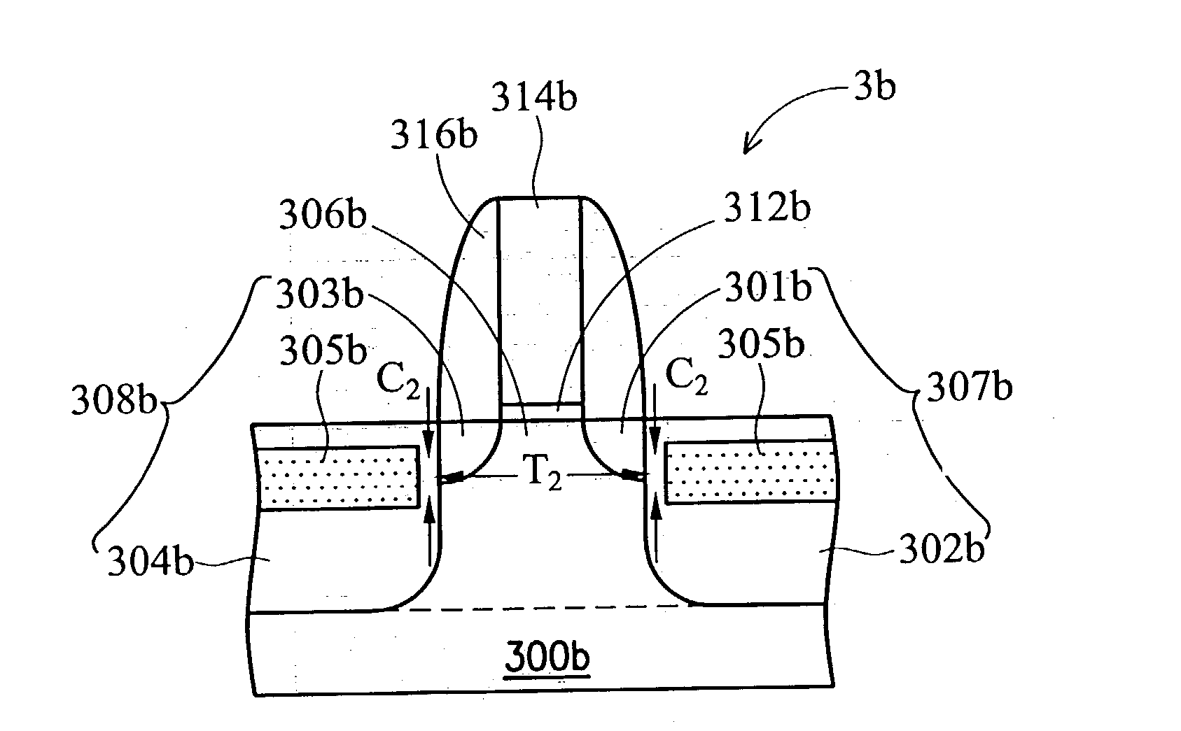
[0029] In the present invention, two kinds of stress modes exerted on the strained-channel region according to the present invention are discussed.
[0030] In FIG. 3A, a cross section of a strained-channel transistor structure 3a in accordance with the first embodiment of the present invention is shown. Substrate 300a, having a strained channel region 306a in a surface, comprises a semiconductor material. Gate dielectric layer 312a, preferably with a thickness between about 3 and 100 .ANG., is on the strained channel region 306a. Gate electrode 314a is on the gate dielectric layer 312a. Spacer 316a is on a sidewall of gate electrode 314a and covers a part of the surface of substrate 300a. Drain region 307a, comprising drain extension region 301a and deeper drain region 302a, and source region 308a, comprising source extension region 303a and deeper source region 304a, are oppositely adjacent to strained channel region 306a. Lattice-mismatched zone 305a, comprising another semiconducto...
second embodiment
[0035] In the second embodiment of the present invention, different kinds of arrangements of lattice-mismatched zone in drain region and / or source region according to the present invention are discussed. In strained-channel transistor structures 4a through 4d in FIGS. 4A through 4D, relationships among substrate 400, drain extension region 401, deeper drain region 402, drain region 407, source extension region 403, deeper source region 404, source region 408, lattice-mismatched zone 405a / 405b / 405c / 405d, strained channel region 406a / 406b / 406c / 406d, gate dielectric layer 412, gate electrode 414, and spacer 416, the same as those described in the first embodiment of the present invention, are omitted.
[0036] In FIG. 4A, lattice-mismatched zone 405a is arranged near the surface of drain region 407 and / or source region 408, and does not extend into drain extension region 401 and / or source extension region 403. In FIG. 4B, lattice-mismatched zone 405b may protrude from the surface of drain...
third embodiment
[0039] In the third embodiment of the present invention, a fabrication method of a strained-channel transistor structure according to the present invention is described. A flowchart of the fabrication method in accordance with the third embodiment of the present invention is shown in FIG. 5. The subsequent descriptions of the fabrication method in accordance with the third embodiment of the present invention follow the steps in FIG. 5.
[0040] In FIG. 6A, a semiconductor substrate such as a silicon substrate 500 is provided. Silicon substrate 500 comprises a previously formed plurality of isolation regions (not shown) and previously defined plurality of device regions (not shown). For example, the isolation regions may be shallow trench isolation regions. FIGS. 6A through 6F provide a cross-sectional view of one single device region for easy description. Silicon substrate 500 comprises, a channel region 506 in an active surface. Silicon substrate 500 is N-type doped when strained-chan...
PUM
 Abstract
Description
Claims
Application Information


