Semiconductor laser device and method of manufacturing the same

a laser device and semiconductor technology, applied in semiconductor lasers, instruments, record information storage, etc., can solve the problems of increasing the distance between the light-emitting spots of the laser beam, complicated manufacturing steps, and increasing the parts coun

Inactive Publication Date: 2004-09-23
PIONEER CORP
View PDF13 Cites 44 Cited by
  • Summary
  • Abstract
  • Description
  • Claims
  • Application Information

AI Technical Summary

Benefits of technology

[0018] Another object of the present invention is to provide a manufacturing method which allows easy, high-volume fabrication of a semiconductor laser device in which the distance between the light-emitting spots of the laser beams is controlled with high precision.

Problems solved by technology

This means a problem of extremely complicated manufacturing steps, for example, in manufacturing semiconductor laser devices intended for an optical pickup.
This produces the problem that the position of emission of the laser beam from the GaN-based laser part (the position of the light-emitting spot) and the positions of emission of the laser beams from the AlGaInP-based and AlGaAs-based laser parts (the positions of the light-emitting spots) are wide apart.
In short, there occurs the problem that the distance between the light-emitting spots of the laser beams increases.
This, however, produces such problems as an increased parts count.

Method used


Image

  • Semiconductor laser device and method of manufacturing the same
  • Semiconductor laser device and method of manufacturing the same
  • Semiconductor laser device and method of manufacturing the same

Examples


first embodiment

[0080] Now, a more concrete example will be described with reference to FIGS. 5 to 8B.

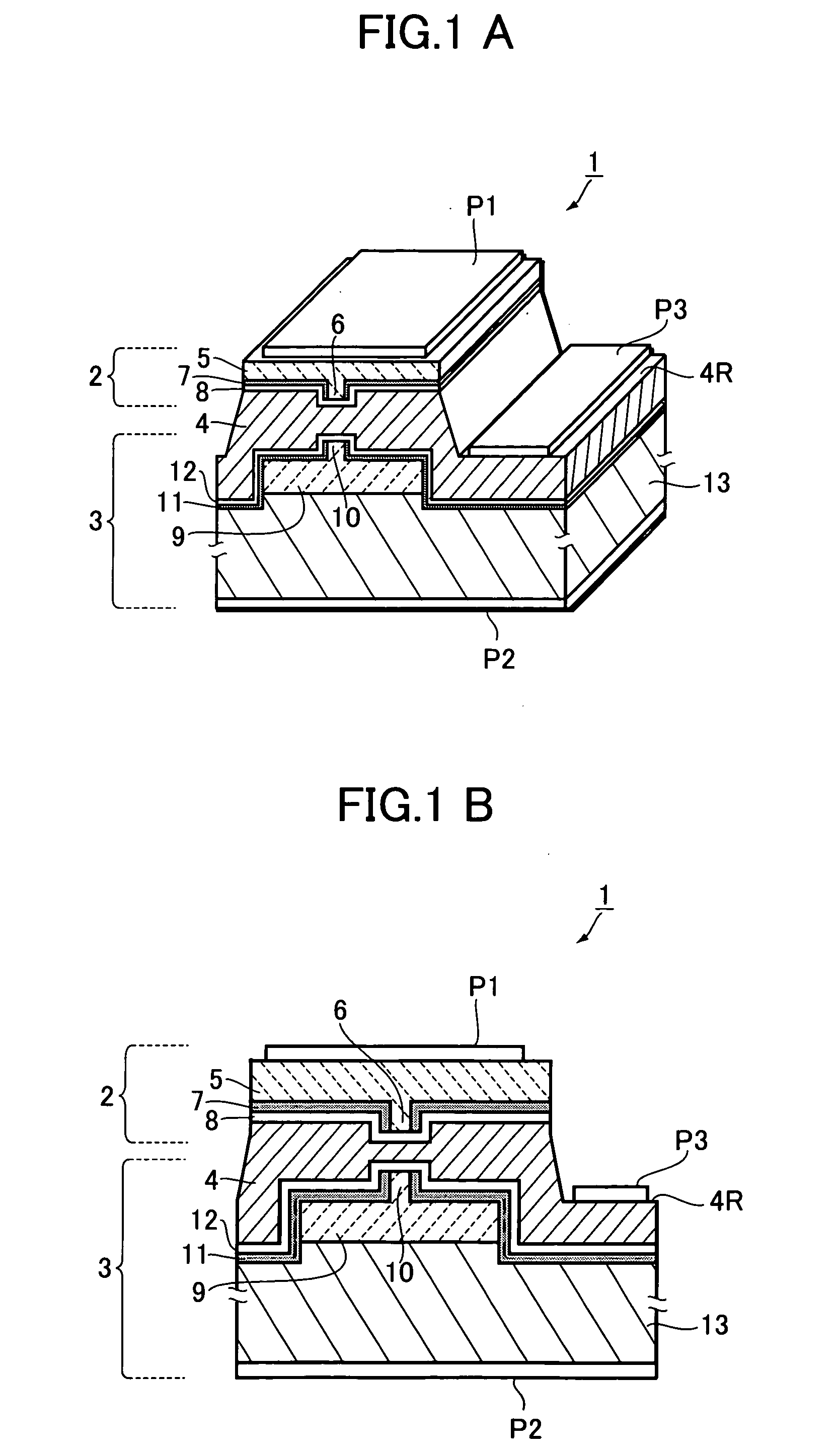
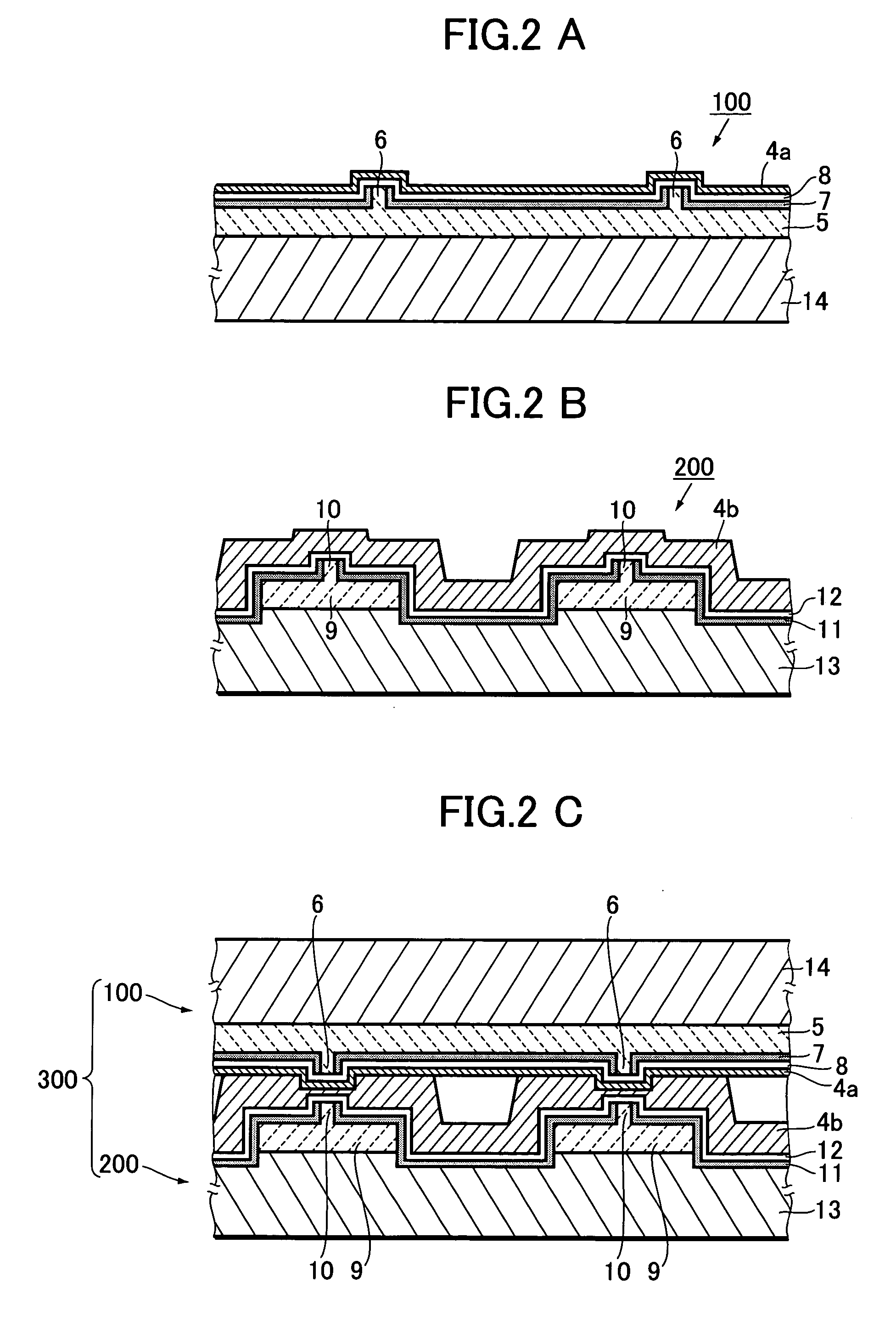
[0081] FIG. 5 is a longitudinal sectional view of a semiconductor laser device in this example, showing the structure thereof in a form corresponding to FIG. 1A. FIGS. 6A to 8B are diagrams showing the steps for manufacturing the semiconductor laser device. Incidentally, in FIGS. 5 to 8B, the parts identical or equivalent to those of FIGS. 1A to 3B are designated by the same reference numerals.

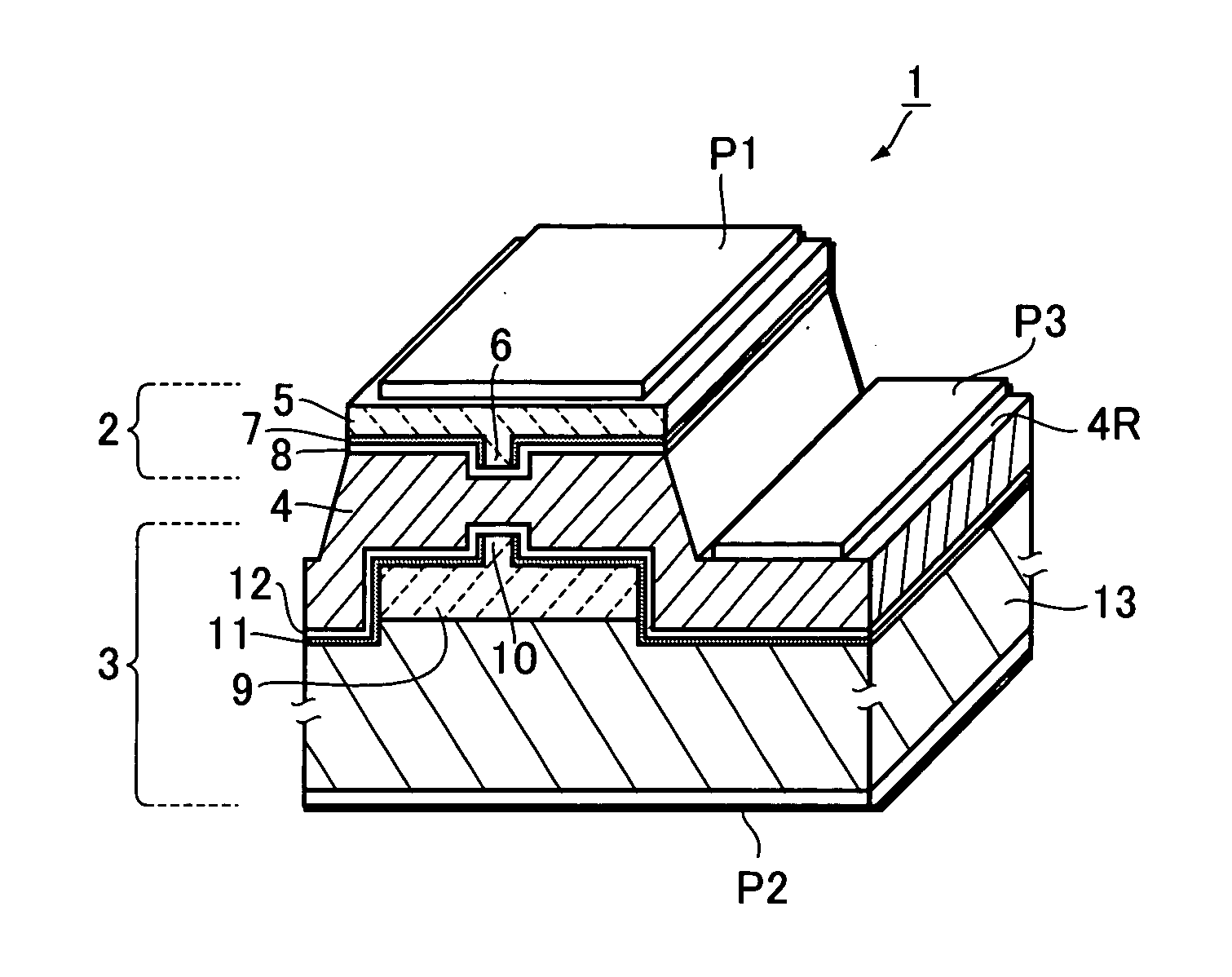
[0082] In FIG. 5, the semiconductor laser device 1 of this example has a hybrid structure in which a first light-emitting element 2, or a GaN-based laser (405-nm-band laser), and a second light-emitting element 3, or an AlGaInP-based laser (650-nm-band laser), are integrally bonded to each other by an adhesive metal layer 4.

[0083] The first light-emitting element 2 includes a laser part 5 which has a ridge waveguide 6. The second light-emitting element 3 includes a laser part 9 which is formed on an n-type G...

second example

[0134] Next, a second example according to the first embodiment will be described with reference to FIG. 9. FIG. 9 is a longitudinal sectional view showing the structure of the semiconductor laser device of this example, in which the parts identical or equivalent to those of FIG. 5 are designated by the same reference numerals.

[0135] In FIG. 9, this semiconductor laser device corresponds to a modified example of the first example, having the structure that the semiconductor laser device 1 shown in FIG. 5 is bonded to an electrically-insulative support substrate (submount) 400 of ceramic or the like having high thermal conductivity.

[0136] The support substrate 400 has a step. An adhesive metal layer P11 and an adhesive metal layer P31 are formed on the lower face (hereinafter, referred to as "first face") and the upper face (hereinafter, referred to as "second face"), respectively.

[0137] The difference in height between the first and second faces is rendered almost the same as the di...

second embodiment

[0147] Now, a second embodiment of the present invention will be described with reference to FIGS. 10A to 12C.

[0148] FIG. 10A is a perspective view showing the external structure of a semiconductor laser device according to the present embodiment. FIG. 10B is a diagram showing the cross-sectional structure of the semiconductor laser device shown in FIG. 10A. FIGS. 11A to 12C are diagrams showing the steps for manufacturing this semiconductor laser device. Incidentally, in FIGS. 10A to 12C, the parts identical or equivalent to those of FIGS. 1A to 3B are designated by the same reference numerals.

[0149] In FIGS. 10A and 10B, this semiconductor laser device 1 has a hybrid structure as in the first embodiment. That is, a first light-emitting element 2 having a laser part 5 for emitting a blue or ultraviolet (short-wavelength) laser beam and a second light-emitting element 3 having a laser part 9 for emitting a laser beam of longer wavelength (for example, in a 600- to 700-nm waveband) a...


PUM


Abstract

A semiconductor laser device comprises: a first light-emitting element having a first laser part, an insulating layer, and an ohmic electrode layer; and a second light-emitting element having a second laser part, an insulating layer, and an ohmic electrode layer. The first laser part has a ridge waveguide, and is formed by stacking thin films of group-III nitride compound semiconductors (for example, GaN-based semiconductors). The second laser part has a ridge waveguide, and is formed by stacking thin films of group III-V compound semiconductors (such as GaAs). The first laser part and the second laser part are integrally bonded to each other by the interposition of an adhesive metal layer which is formed between the ohmic electrode layers. This provides the semiconductor laser device with a small distance between the light-emitting spots of the laser parts.

Description

[0001] 1. Field of the Invention[0002] The present invention relates to a semiconductor laser device for emitting a plurality of laser beams having different wavelengths and a method of manufacturing the same.[0003] The present application claims priority from Japanese Patent Application No. 2002-374635, the disclosure of which is incorporated herein by reference in its entirety.[0004] 2. Description of the Related Art[0005] In recent years, a semiconductor laser device called multi-wavelength laser for emitting a plurality of laser beams having different wavelengths has been under research and development.[0006] For example, in the field of data recording and reproducing apparatuses with storage media called optical discs, typified by CDs (Compact Discs), DVDs (Digital Versatile Discs), etc., it has been of importance to develop a semiconductor laser device which can emit a plurality of laser beams having different wavelengths. The aim is to develop an optical pickup which has comp...

Claims


Application Information

Patent Timeline
Patent Type & Authority Applications(United States)
IPC IPC(8): H01S5/22H01S5/02H01S5/042H01S5/323H01S5/343H01S5/40
CPCB82Y20/00H01S2304/04G11B2007/0006H01S5/0202H01S5/0207H01S5/0213H01S5/0217H01S5/0224H01S5/02272H01S5/02461H01S5/0421H01S5/0425H01S5/2214H01S5/2231H01S5/32325H01S5/32341H01S5/34326H01S5/34333H01S5/4043H01S5/4087H01S2301/173G11B7/1275H01L2224/48463H01S5/04256H01S5/0237H01S5/0234
Inventor MIYACHI, MAMORUWATANABE, ATSUSHITAKAHASHI, HIROKAZUKIMURA, YOSHINORI
Owner PIONEER CORP
Why Eureka
Try Eureka