
Eureka
For R&D, Eureka makes reading and utilizing patents & technical documents easy.
Eureka AIR
Designed for self-driven R&D workflows. Generate viable solutions, solve complex R&D challenges, empower your innovation with AI.

Eureka Materials
Designed for material experts only. Revolutionize your material R&D, from search, analyze, to developing new materials.

TechResearch
Generate reliable direction feasibility study reports for your R&D in just a few steps.

TechSeek
Discover and master advanced knowledge NOW. Basics, ideas, possibilities, all at once.

TechMind
As an expert in R&D Theories, TechMind can generates customized viable solutions instantly.

TechRisk
Analyze your overall solution with one click, know your potential R&D risks in advance.

TechMonitor
Get weekly tech updates, stay abreast of the latest tech innovations and key insights.
Scratch masking coatings for optical substrates
- Summary
- Abstract
- Description
- Claims
- Application Information
AI Technical Summary
Benefits of technology
Problems solved by technology
Method used
Image

Examples
example 1
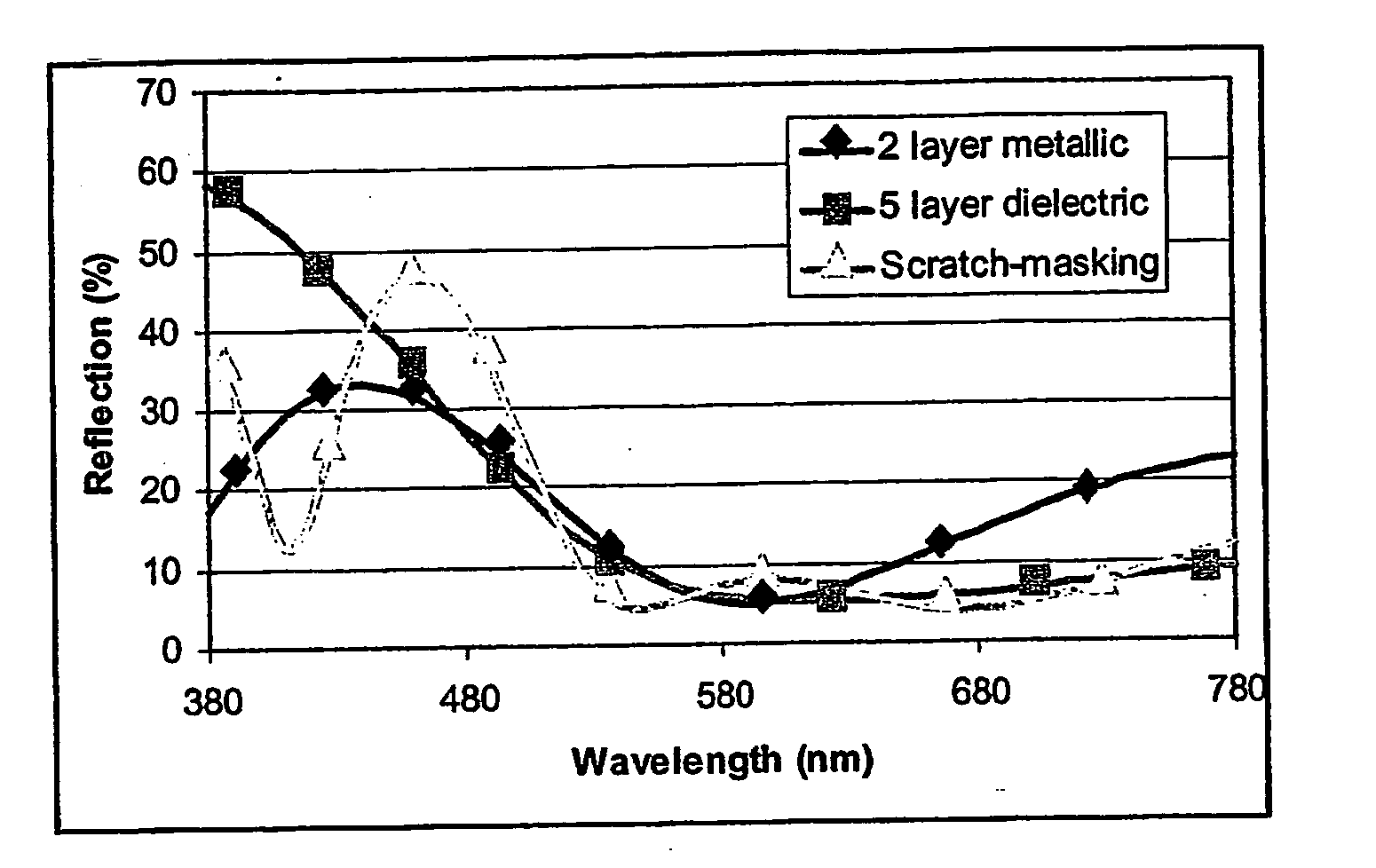
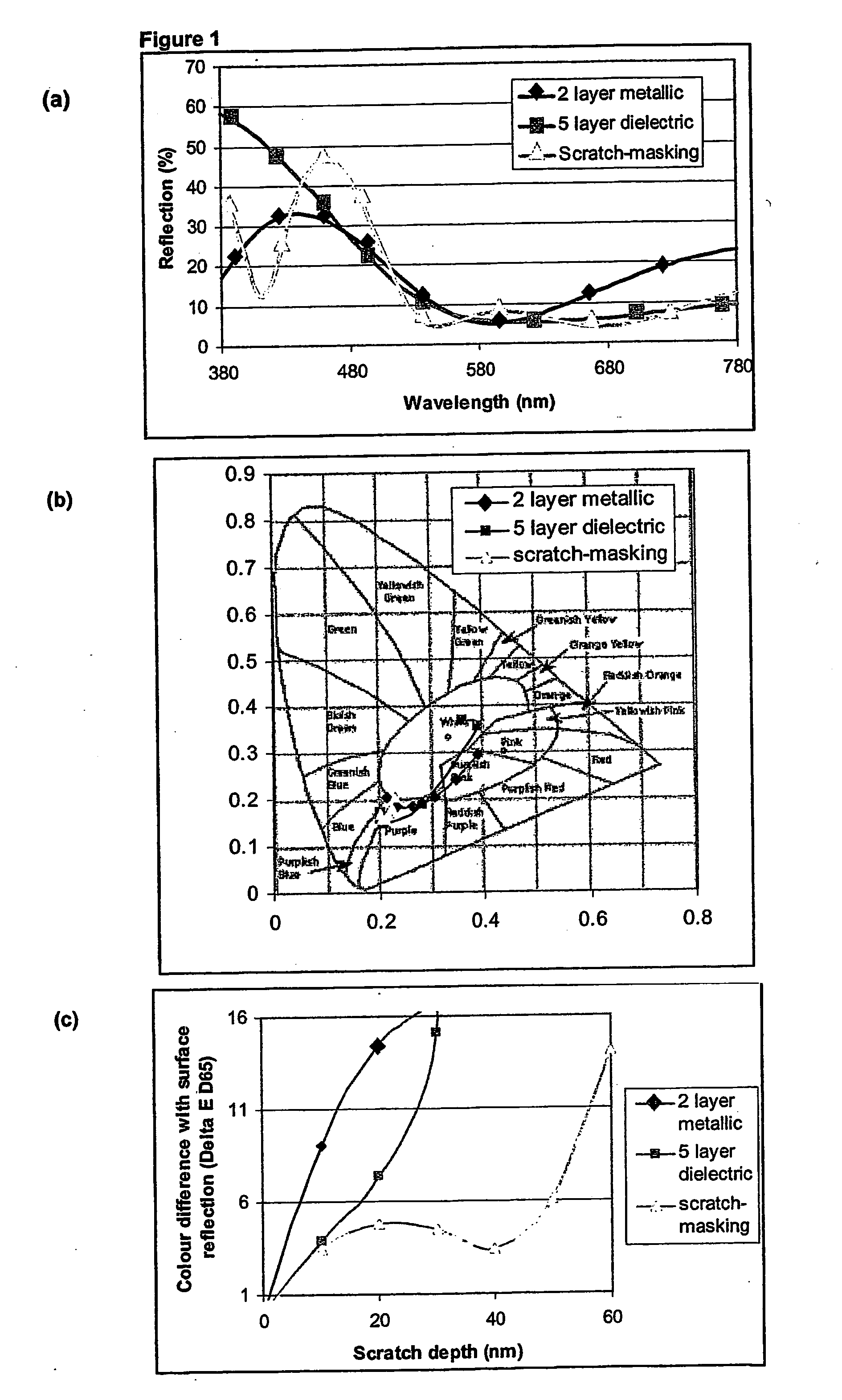
[0056] Table 1 illustrates an example of a scratch resistant, night blue reflective (mirror) coating and two comparative coatings with similar reflectance and colour characteristics (as determined using the CIE 1931 colour system). The first comparative coating is a two layer metallic coating. The second comparative coating is a five layer dielectric coating.
[0057] The properties of each of the coatings is as calculated using the commercial software package Tfcalc (Thin Film Design software by Software Spectra Inc, Portland Oreg., USA).
1 TABLE 1 2 layer 5 layer Scratch -Thickness (nm) metallic dielectric masking Cr 5 0 0 SiO.sub.2 295 242 0 Material with 0 50 37 n = 2.09@550 nm SiO.sub.2 0 51 57 Material with 0 32 178 n = 2.09@550 nm Top SiO.sub.2 0 20 317 R (%) 10.6 9.9 9.9 x (CIE1931) 0.213 0.201 0.201 y (CIE 1931) 0.203 0.167 0.169 The term "R" represents the predicted percentage luminosity of the light reflected from the coating. Values x and y represent predicted chromaticity c...
example 2
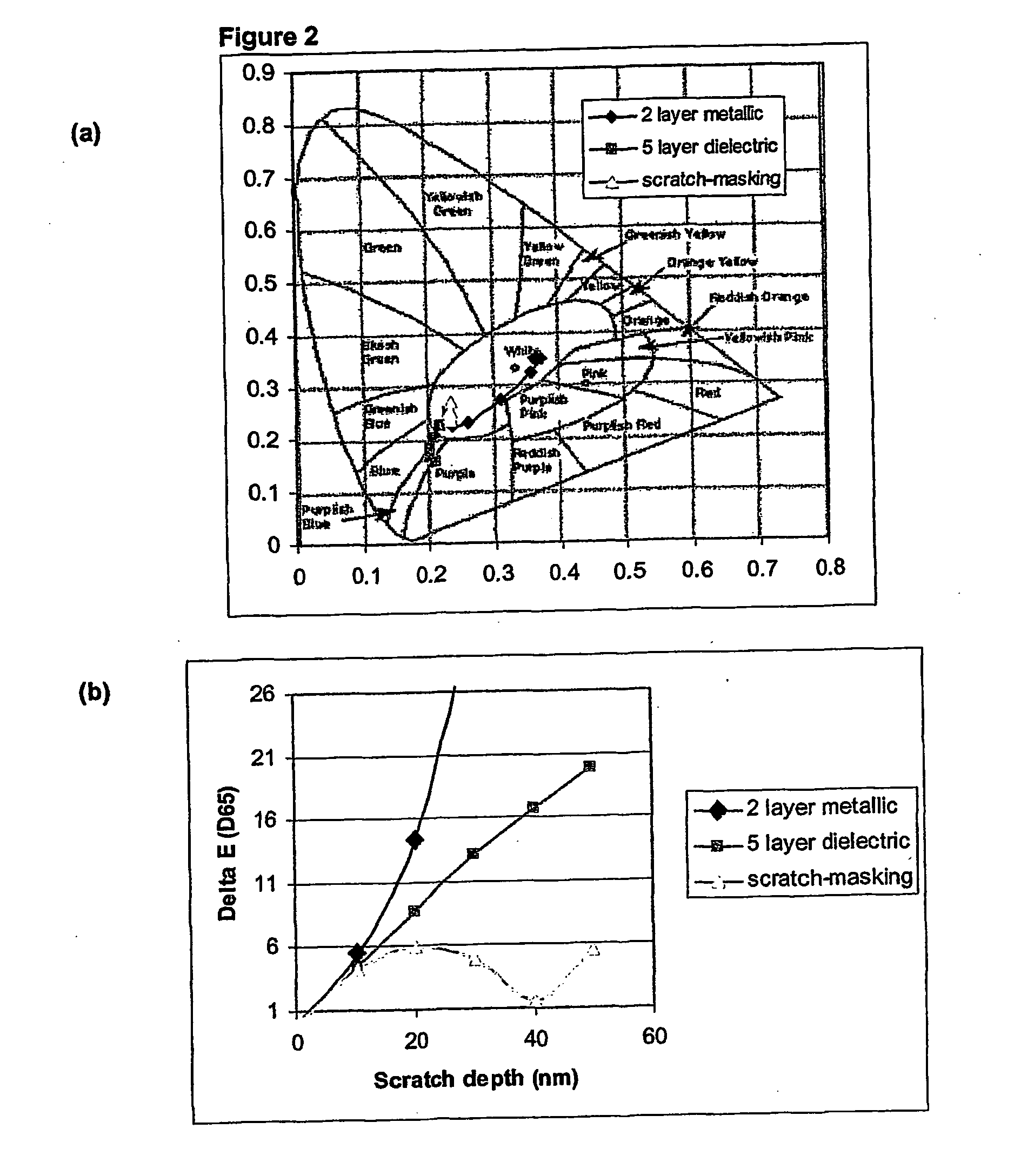
[0063] Table 2 illustrates an example of a scratch resistant, sky blue reflective (mirror) coating and two comparative coatings with similar reflectance and colour characteristics (as determined using the CIE 1931 system of colour specification). The first comparative coating is a two layer metallic coating. The second comparative coating is a five layer dielectric coating.
[0064] The properties of each of the coatings is as calculated using the commercial software package Tfcalc (Thin Film Design software by Software Spectra Inc, Portland Oreg., USA).
2 TABLE 2 2 layer 5 layer Scratch -Thickness (nm) metallic dielectric masking Cr 5 0 0 SiO.sub.2 100 73 48.2 Material with 0 39.9 164.8 n = 2.09 @ 550 nm SiO.sub.2 0 75.3 117.3 Material with 0 14.6 146.6 N = 2.09 @ 550 nm Top SiO.sub.2 0 69 327.7 R (%) 7.6 14.4 14.4 x (CIE1931) 0.235 0.230 0.230 y (CIE 1931) 0.223 0.249 0.250 The term "R" represents the predicted percentage luminosity of the light reflected from the coating. Values x an...
example 3
[0070] Table 3 illustrates an example of a scratch resistant, black reflective (mirror) coating and two comparative coatings with similar reflectance and colour characteristics (as determined using the CIE 1931 system of colour specification). The first comparative coating is a two layer metallic coating. The second comparative coating is a, five layer dielectric coating.
[0071] The properties of each of the coatings is as calculated using the commercial software package Tfcalc (Thin Film Design software by Software Spectra Inc, Portland Oreg., USA).
3 TABLE 3 2 layer 5 layer Scratch -Thickness (nm) metallic dielectric masking Cr 5 0 0 SiO.sub.2 70 0 50 Material with 0 17.8 10 n = 2.09@550 nm SiO.sub.2 0 39.6 54.9 Material with 0 50.9 25.2 n = 2.09@550 nm Top SiO.sub.2 0 187 21.7 R (%) 7.6 15.6 13.4 x (CIE1931) 0.355 0.307 0.323 y (CIE 1931) 0.325 0.316 0.320 The term "R" represents the predicted percentage luminosity of the light reflected from the coating. Values x and y represent p...
PUM
 Abstract
Description
Claims
Application Information
 - R&D Engineer
- R&D Manager
- IP Professional
- Industry Leading Data Capabilities
- Powerful AI technology
- Patent DNA Extraction
Browse by: Latest US Patents, China's latest patents, Technical Efficacy Thesaurus, Application Domain, Technology Topic, Popular Technical Reports.
© 2024 PatSnap. All rights reserved.Legal|Privacy policy|Modern Slavery Act Transparency Statement|Sitemap|About US| Contact US: help@patsnap.com