Semiconductor device and production method for semiconductor device

Inactive Publication Date: 2015-01-15
FUJI ELECTRIC CO LTD
View PDF4 Cites 17 Cited by
  • Summary
  • Abstract
  • Description
  • Claims
  • Application Information

AI Technical Summary

Benefits of technology

[0023]According to the semiconductor device and the semiconductor device producing method of the invention, it is possible to reduce a high-temperature reverse leakage current when the reverse voltage is applied, to improve the trade-off relationship between turn-off l

Problems solved by technology

As a result, the operation temperature (heat resistance) of the element is limited.
Therefore, it is difficult to maint

Method used


Image

  • Semiconductor device and production method for semiconductor device
  • Semiconductor device and production method for semiconductor device
  • Semiconductor device and production method for semiconductor device

Examples


embodiment

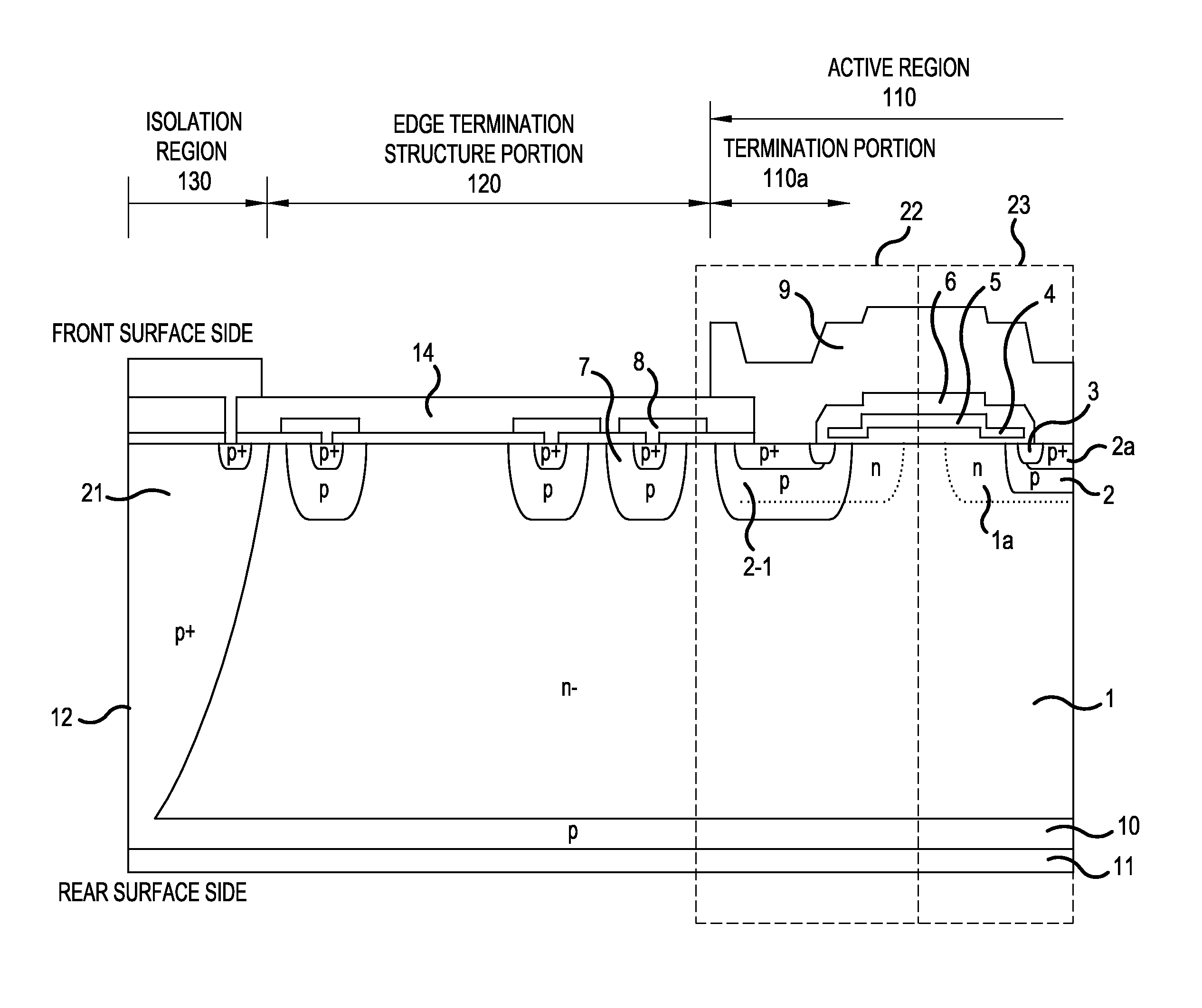
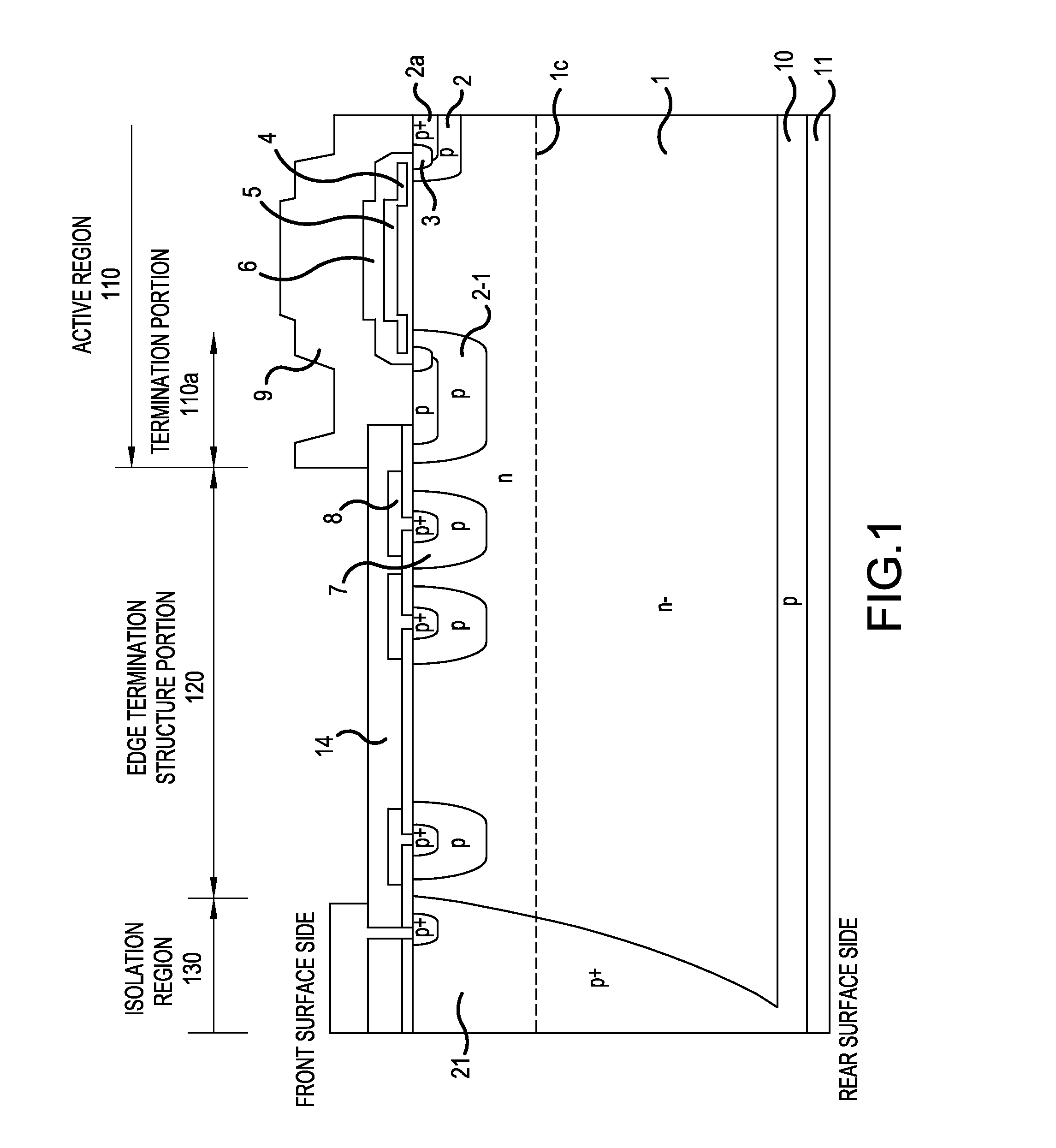
[0040]A reverse blocking IGBT will be described as an example of a reverse blocking semiconductor device according to an embodiment of the invention. FIG. 1 is a cross-sectional view illustrating the structure of a main portion of the reverse blocking IGBT according to the embodiment of the invention. As illustrated in FIG. 1, the reverse blocking IGBT according to the embodiment includes an active region 110 which is provided in the vicinity of the center of a chip, an edge termination structure portion 120 which is provided in the outer circumference surrounding the active region 110, and a isolation region 130 which surrounds the outside of the edge termination structure portion 120. The isolation region 130 includes, as a main region, a p+ isolation layer 21 for connecting one main surface and the other main surface of an n− semiconductor substrate with a p-type region. That is, the p+ isolation layer 21 is provided so as to pass through the n− semiconductor substrate in a depth...


PUM


Abstract

Depth of a termination p base region provided in a termination portion of an active region close to an edge termination structure portion is more than depth of a p-type base region provided inside the termination p base region. An n-type high-concentration region is provided from one main surface of the semiconductor substrate in the entire surface layer of one surface of a semiconductor substrate within a depth of 20 μm or less below the bottom of the termination p base region. Ratio of the impurity concentration n1 of the n-type high-concentration region (1c) to the impurity concentration n2 of an n drift region satisfies 1.0<n1/n2≦5.0. Reverse leakage current when operation temperature of an element is high can be reduced and trade-off between on-state voltage and switching loss can be improved. Rising peak voltage of collector voltage when a semiconductor device is off is reduced.

Description

BACKGROUND OF THE INVENTION[0001]A. Field of the Invention[0002]The present invention relates to a reverse blocking IGBT which can improve a trade-off relationship among a reverse leakage current at a reverse breakdown voltage, an on-state voltage, and switching loss and a method for producing the same.[0003]B. Description of the Related Art[0004]A high-breakdown-voltage discrete power device plays a key role in a power conversion device. Examples of the power device include an insulated gate bipolar transistor (IGBT) and a MOS gate (metal-oxide-semiconductor insulated gate) field effect transistor (MOSFET). The IGBT is a conductivity-modulation-type bipolar device and has a lower on-state voltage than the MOSFET which is a unipolar device. Therefore, in general, the IGBT is particularly applied to a high-breakdown voltage device for switching in which the on-state voltage is likely to be high.[0005]When a matrix converter with high conversion efficiency is used as the power convers...

Claims


Application Information

Patent Timeline
IPC IPC(8): H01L29/739H01L21/225H01L21/265H01L29/06H01L29/66
CPCH01L29/0646H01L29/66325H01L21/225H01L21/265H01L29/7393H01L21/761H01L29/1095H01L29/66333H01L29/7395H01L29/7397H01L29/42368H01L29/404H01L29/0834H01L29/0847H01L29/0619H01L21/2255H01L21/26513H01L29/36
Inventor LU, HONG-FEI
Owner FUJI ELECTRIC CO LTD
Why Eureka
Try Eureka