Narrow fin finfet

a technology of narrow fins and fins, which is applied in the direction of semiconductor devices, electrical equipment, transistors, etc., can solve the problems of conventional mosfets that have difficulty scaling below 50 nm fabrication processing

Inactive Publication Date: 2004-10-07
GLOBALFOUNDRIES US INC
View PDF19 Cites 82 Cited by
  • Summary
  • Abstract
  • Description
  • Claims
  • Application Information

AI Technical Summary

Problems solved by technology

Conventional MOSFETs have difficulty scaling below 50 nm fabrication processing.

Method used


Image

  • Narrow fin finfet
  • Narrow fin finfet
  • Narrow fin finfet

Examples


Embodiment Construction

refers to the accompanying drawings. The same reference numbers may be used in different drawings to identify the same or similar elements. Also, the following detailed description does not limit the invention. Instead, the scope of the invention is defined by the appended claims and equivalents.

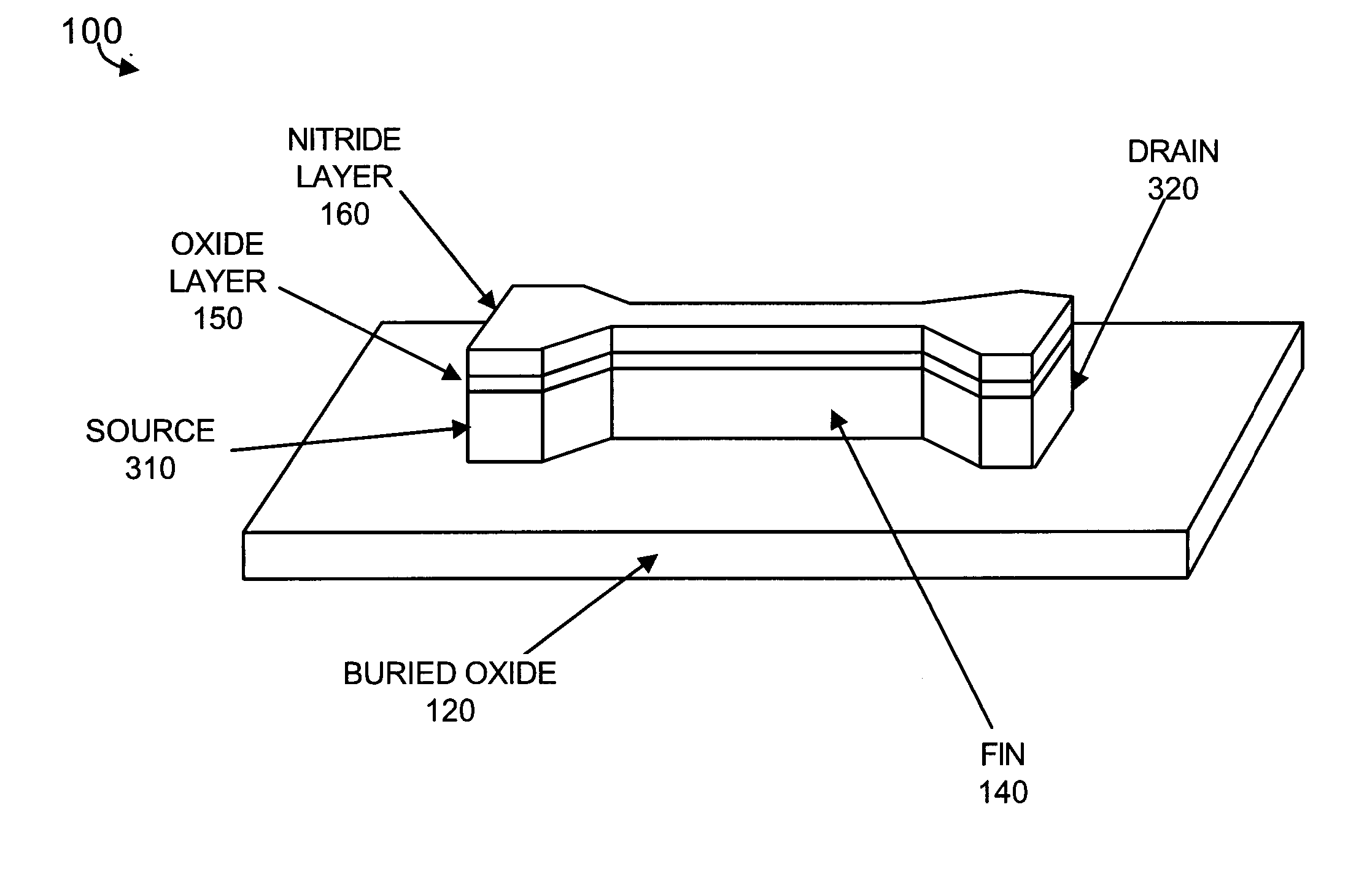
[0023] A FinFET, as the term is used herein, refers to a type of MOSFET in which a conducting channel is formed in a vertical Si "fin." FinFETs are generally known in the art.

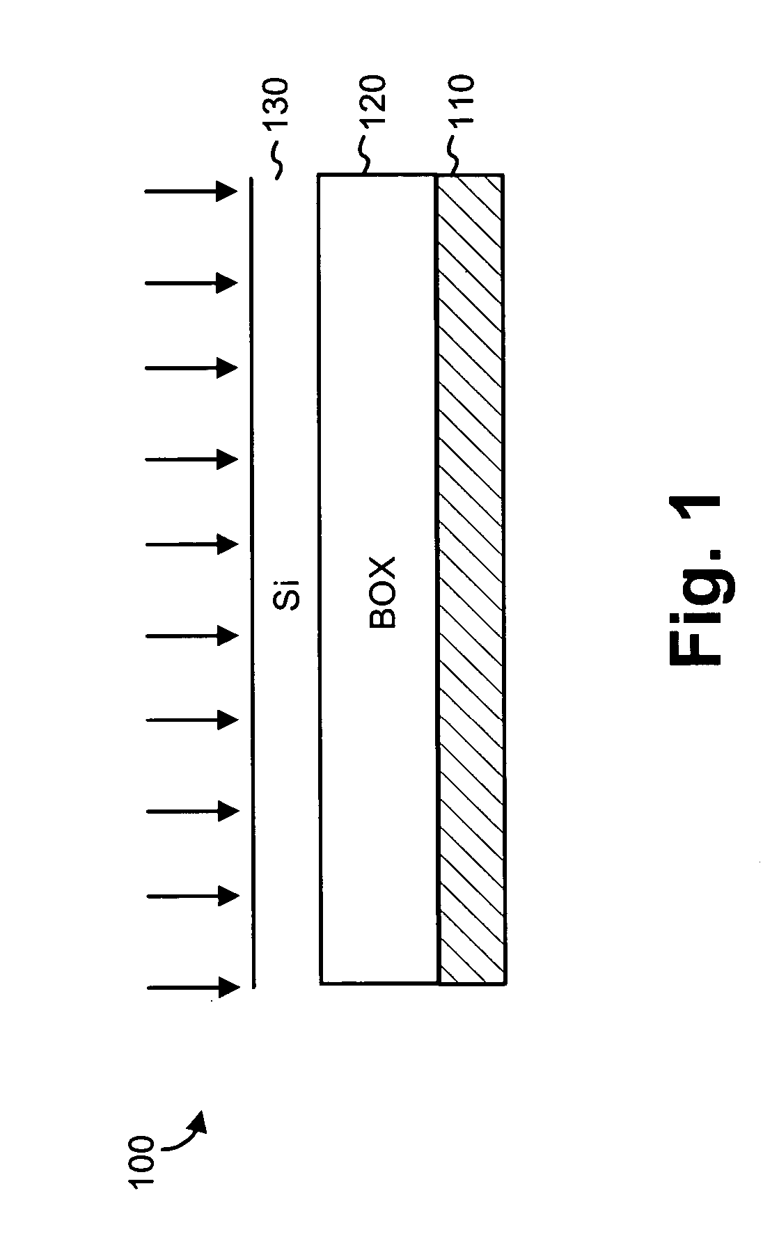
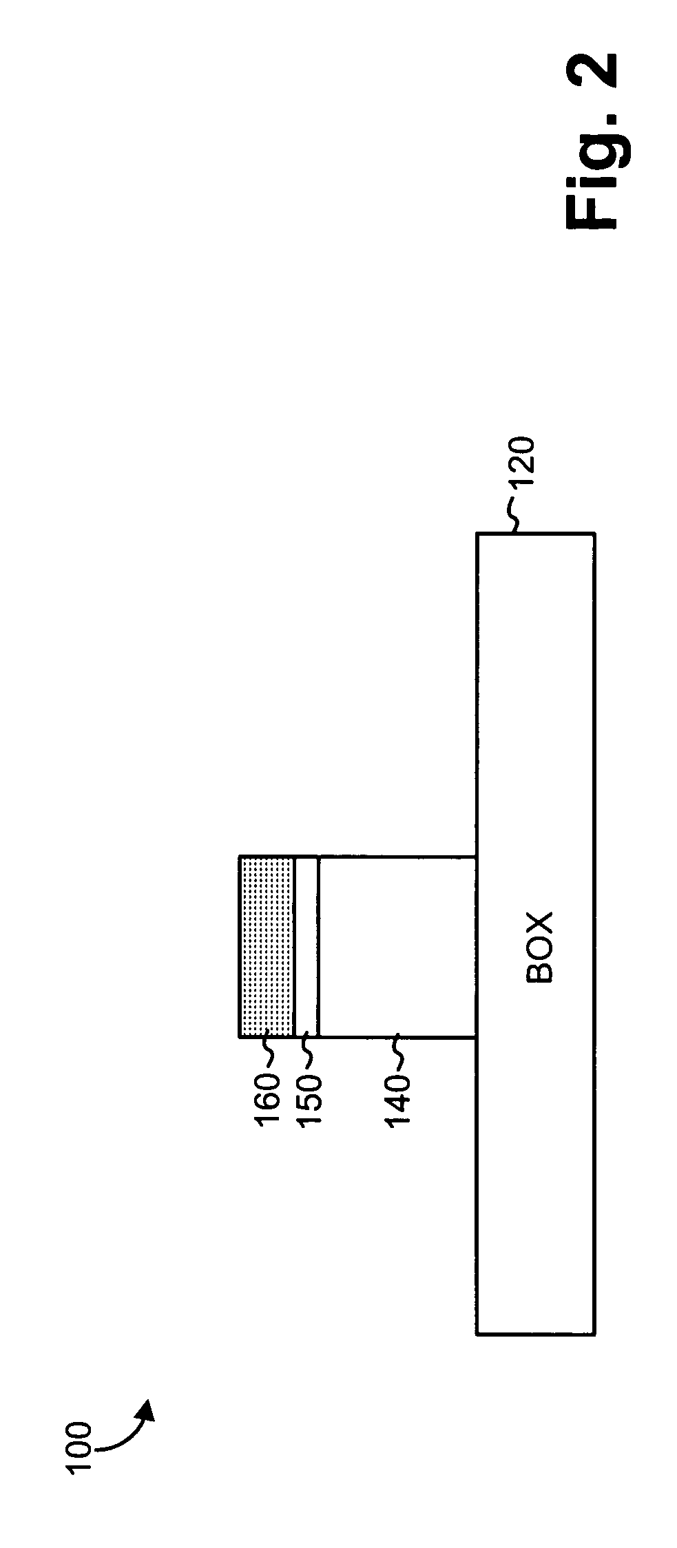
[0024] FIG. 1 is a cross-section illustrating doping of a starting structure for a FinFET 100. FinFET 100 may include a silicon-on-insulation (SOI) structure that includes buried oxide (BOX) layer 120 formed on a silicon and / or germanium substrate 110, with a silicon layer 130 over BOX layer 120. Alternatively, layer 130 may comprise germanium or silicon-germanium. In an exemplary implementation, BOX layer 120 may have a thickness ranging from about 200 nm to about 400 nm and silicon layer 130 may have a thickness rangi...


PUM


Abstract

A narrow channel FinFET is described herein with a narrow channel width. A protective layer may be formed over the narrow channel, the protective layer being wider than the narrow channel.

Description

[0001] A. Field of the Invention[0002] The present invention relates generally to semiconductor devices and methods of manufacturing semiconductor devices and, more particularly, to double-gate metal oxide semiconductor field-effect transistors (MOSFETs).[0003] B. Description of Related Art[0004] Transistors, such as MOSFETs, are the core building block of the vast majority of semiconductor devices. Some semiconductor devices, such as high performance processors, can include millions of transistors. For these devices, decreasing transistor size, and thus increasing transistor density, has traditionally been a high priority in the semiconductor manufacturing area.[0005] Conventional MOSFETs have difficulty scaling below 50 nm fabrication processing. To develop sub-50 nm MOSFETs, double-gate MOSFETs have been proposed. In several respects, double-gate MOSFETs offer better characteristics than the conventional bulk silicon MOSFETs. These improvements arise because the double-gate MOSFE...

Claims


Application Information

Patent Timeline
Patent Type & Authority Applications(United States)
IPC IPC(8): H01L21/336H01L29/423H01L29/786
CPCH01L29/42384H01L29/78687H01L29/785H01L29/66818
Inventor KRIVOKAPIC, ZORANAN, JUDY XILINDAKSHINA-MURTHY, SRIKANTESWARAWANG, HAIHONGYU, BIN
Owner GLOBALFOUNDRIES US INC
Why Eureka
Try Eureka