Reduction of negative bias temperature instability in narrow width PMOS using F2 implantation

a technology of implantation and temperature instability, which is applied in the direction of basic electric elements, electrical apparatus, and semiconductor devices. it can solve the problems of difficult to achieve the high density of these complex integrated circuits, limiting factors of negative bias temperature instability (nbti), and knobs sometimes used to reduce nbti

Inactive Publication Date: 2004-08-24
INFINEON TECH AG
View PDF45 Cites 28 Cited by
  • Summary
  • Abstract
  • Description
  • Claims
  • Application Information

AI Technical Summary

Benefits of technology

Another object of the present invention is to provide a process to suppress negative bias temperature instability in narrow width PMOSFET devices by the use of sidewall fluorine implantation.
A further object of the present invention is to provide a process to suppress negative bias temperature instability in narrow width PMOSFET devices by introducing sidewall fluorine implantation after shallow trench isolation (STI) liner oxidation and before STI HDP fill, by implanting fluorine through the STI liner.

Problems solved by technology

The high density of these complex integrated circuits are not easily achieved by decreasing a layout according to device proportions of the integrated circuits.
In the case of producing PMOSFET microelectronic devices, negative bias temperature instability (NBTI) is a limiting factor insofar as the reliability of the PMOSFET is concerned.
The basic cause of NBTI remains unknown, and knobs sometimes used to reduce NBTI are very limited.
This being the case, the allowable change of fluorine dose is very limited.
Unfortunately, this limit severely restricts the ability to reduce NBTI.
Accordingly, these traditional techniques are not very efficient in introducing fluorine into Si / SiO.sub.2 interface.
It is known that narrow channel width devices exhibit higher NBTI / NBTS than wider channel devices for the same channel length; however, there is no known solution to this problem.
While this technique is good enough for wider channel length devices, it is not good enough for narrow channel width devices.
This is in part due to the fact that, as gate oxide thicknesses get thinner, the amount of fluorine introduced through the source / drain implant is not enough for wider channel length devices--let alone narrow channel width devices.

Method used


Image

  • Reduction of negative bias temperature instability in narrow width PMOS using F2 implantation
  • Reduction of negative bias temperature instability in narrow width PMOS using F2 implantation

Examples


Embodiment Construction

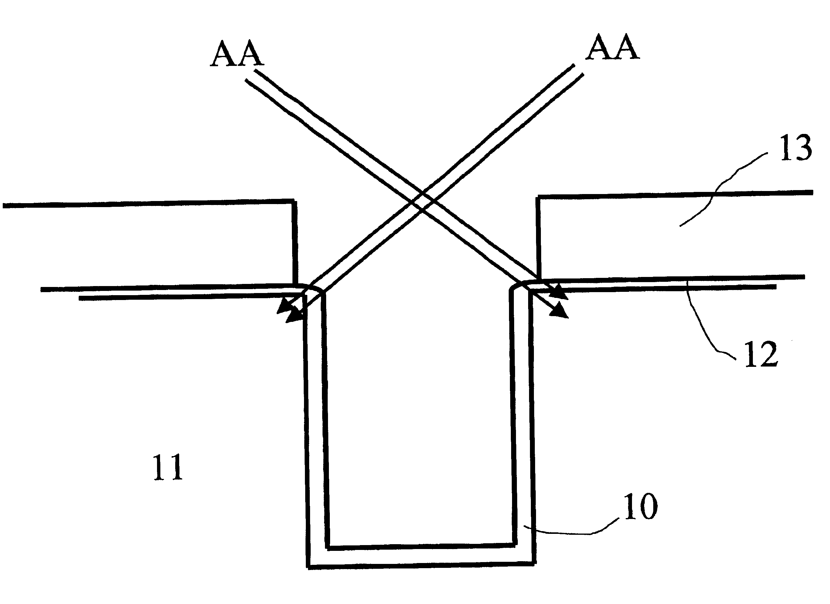
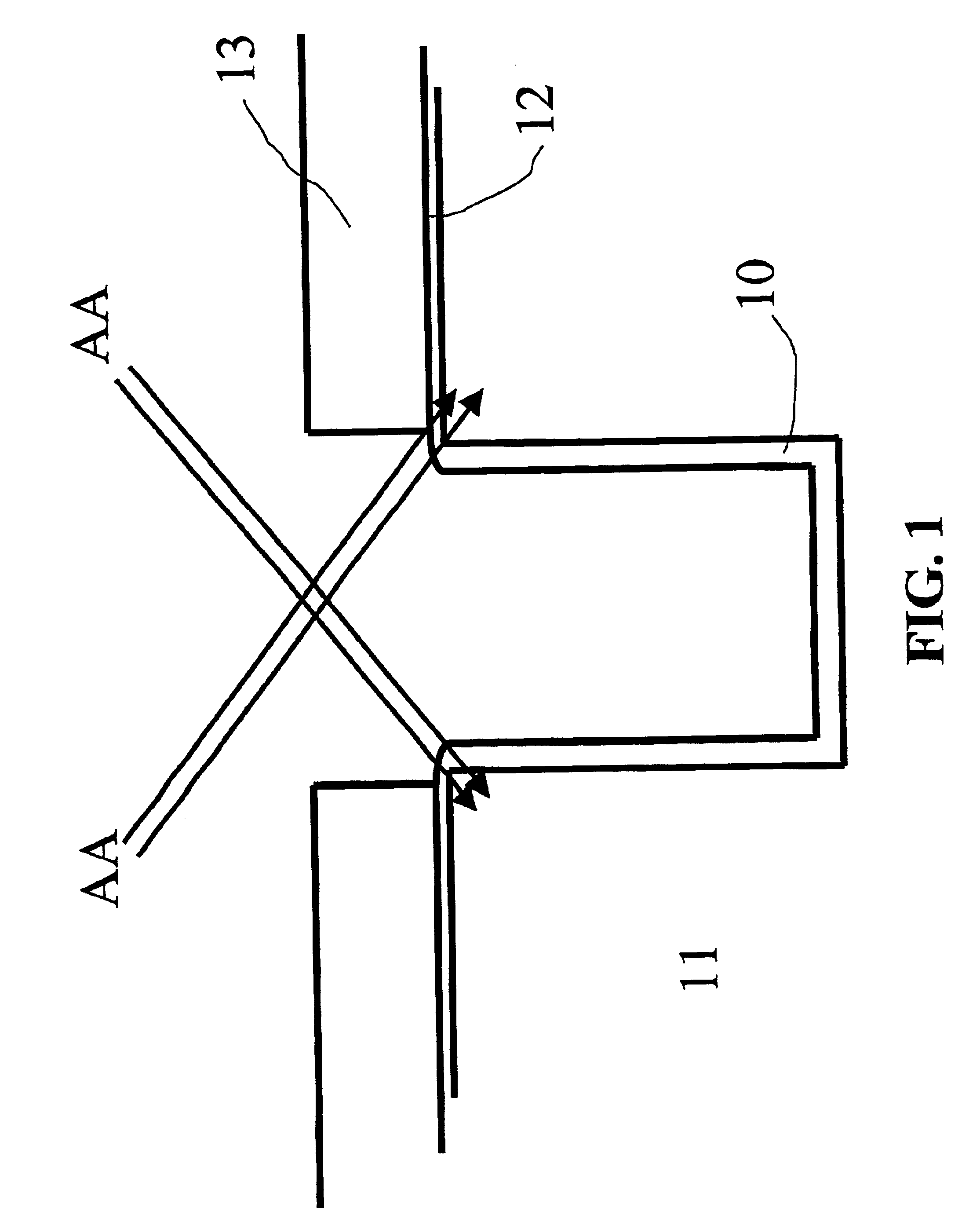
The fabrication of MOSFET devices are well known. For example, MOSFETs are manufactured by placing an undoped polycrystalline (polysilicon) material over a thin gate oxide, whereupon the polysilicon material and gate oxide are patterned to form a gate conductor with source / drain regions adjacent to and on opposite sides of the gate conductor. Thereafter, the gate conductor and source / drain regions are implanted with an impurity dopant material. In the case where the impurity dopant material used for forming the source / drain regions is n-type the resulting MOSFET is an NMOSFET (n-channel) transistor device. On the other hand, if the source / drain impurity dopant material is p-type, the resulting MOSFET is a PMOSFET (p-channel) transistor device.

The gate conductor and adjacent source / drain regions are produced using well-known photolithography techniques. The gate conductors and source / drain regions generally arise in openings formed through a thick layer known as a field oxide. These ...


PUM


Abstract

In a process of fabricating a narrow channel width PMOSFET device, the improvement of affecting reduction of negative bias temperature instability by use of F2 side wall implantation, comprising:a) forming a shallow trench isolation (STI) region in a substrate;b) forming a gate on a gate oxide in the substrate;c) forming a liner layer in said shallow trench isolation region and subjecting the liner layer to oxidation to form a STI liner oxidation layer;d) implanting F2 into side walls of the STI liner oxidation layer at a large tilted angle in sufficient amounts to affect reduction of negative bias temperature instability after a high density plasma fill of the STI F2 implanted liner oxidation layer; ande) filling the STI F2 implanted structure from step d) with a high density plasma (HDP) fill to affect reduction of negative bias temperature instability.

Description

1. Field of the InventionThe invention relates to a process of producing narrow width PMOSFET (p-metal oxide semiconductor field effect transistor) in a manner so as to affect reduction of negative bias temperature instability (NBTI / NBTS). More particularly, the present invention relates to a process to suppress negative bias temperature instability in narrow channel width PMOS devices by implantation of F.sub.2 after STI (shallow trench isolation) liner oxidation and prior to the STI HDP fill.2. Description of Prior ArtAs integrated circuits become more complicated and their function becomes more powerful, the necessary density of transistors in the integrated circuit increases accordingly. The high density of these complex integrated circuits are not easily achieved by decreasing a layout according to device proportions of the integrated circuits. Instead, the device size must be decreased by a design rule and with consideration for potential change in the physical characteristics...

Claims


Application Information

Patent Timeline
Patent Type & Authority Patents(United States)
IPC IPC(8): H01L21/762H01L29/02H01L21/70H01L29/10H01L21/8234H01L21/265H01L21/02
CPCH01L21/76237H01L21/823481H01L29/1033H01L21/26506H01L21/26586H01L21/2658
Inventor LIN, CHUAN
Owner INFINEON TECH AG
Why Eureka
Try Eureka