Semiconductor device

a technology of semiconductor devices and semiconductors, applied in semiconductor devices, semiconductor/solid-state device details, electrical devices, etc., can solve the problems of inability to realize a light-emitting device including a tft directly formed over a substrate, unsuitable mass production of substrates, and fragile and heavy materials,

Inactive Publication Date: 2004-10-28
SEMICON ENERGY LAB CO LTD
View PDF90 Cites 64 Cited by
  • Summary
  • Abstract
  • Description
  • Claims
  • Application Information

AI Technical Summary

Problems solved by technology

As a substrate for forming these TFTs, a glass substrate or a quartz substrate is widely used now, however, these substrates have some drawbacks such as being fragile and heavy.
Further, these substrates are unsuitable for mass-production since it is difficult to use a large-sized glass substrate or a large-sized quartz substrate.
However, the maximum temperature of the

Method used


Image

  • Semiconductor device
  • Semiconductor device
  • Semiconductor device

Examples


embodiment 1

[0042] Embodiment 1

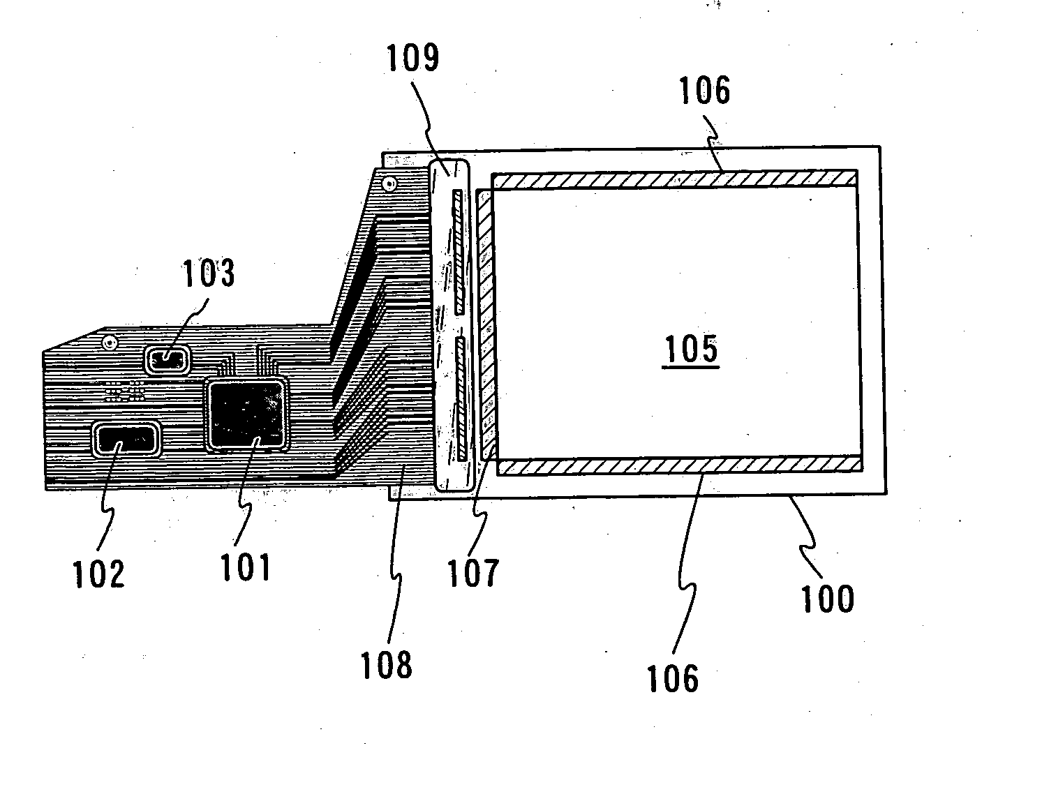
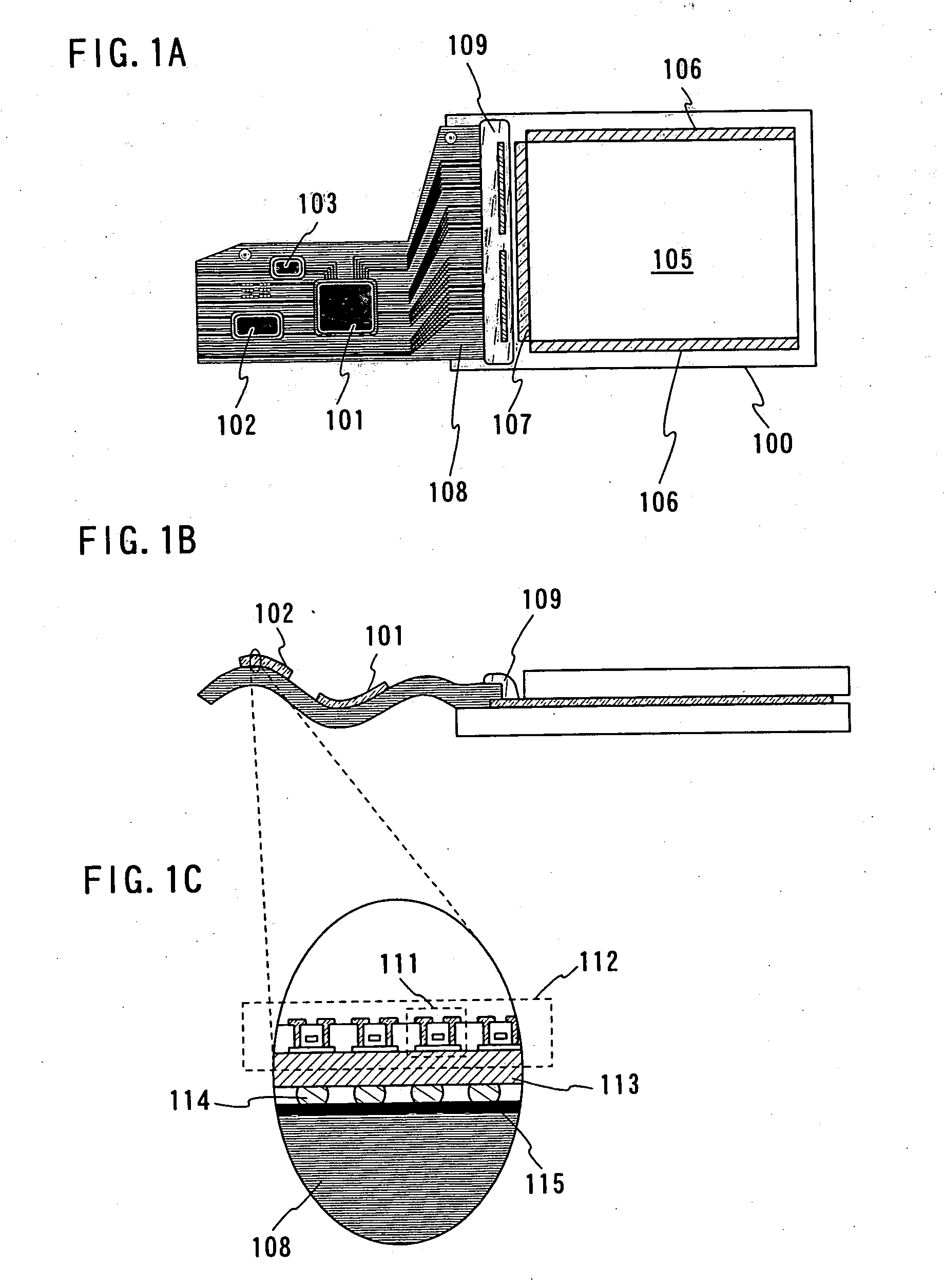
[0043] A module (semiconductor module), which is provided with an integrated circuit formed by a transfer technique over an FPC (Flexible Printed Circuit) for connecting electrically a panel 100 to outside will be explained in this embodiment with reference to FIGS. 1A to 1C.

[0044] FIG. 1A is a top view of a semiconductor module. FIG. 1B is a cross-sectional view of the semiconductor module. The panel 100 is provided with a pixel portion 105 and a driver circuit (a signal line driver circuit 107, a scanning line driver circuit 106). An FPC (Flexible Printed Circuit) 108 for connecting electrically the driver circuit to an external power source or the like provided at outside (not shown) is pasted over the panel 100 with an adhesive 109.

[0045] Further, an integrated circuit (a controller 101, CPU (Central Processing Unit) 102, a memory 103) is formed over the FPC 108 by the transfer technique.

[0046] In addition, the integrated circuit (a controller 101, CPU (Centra...

embodiment 2

[0053] Embodiment 2

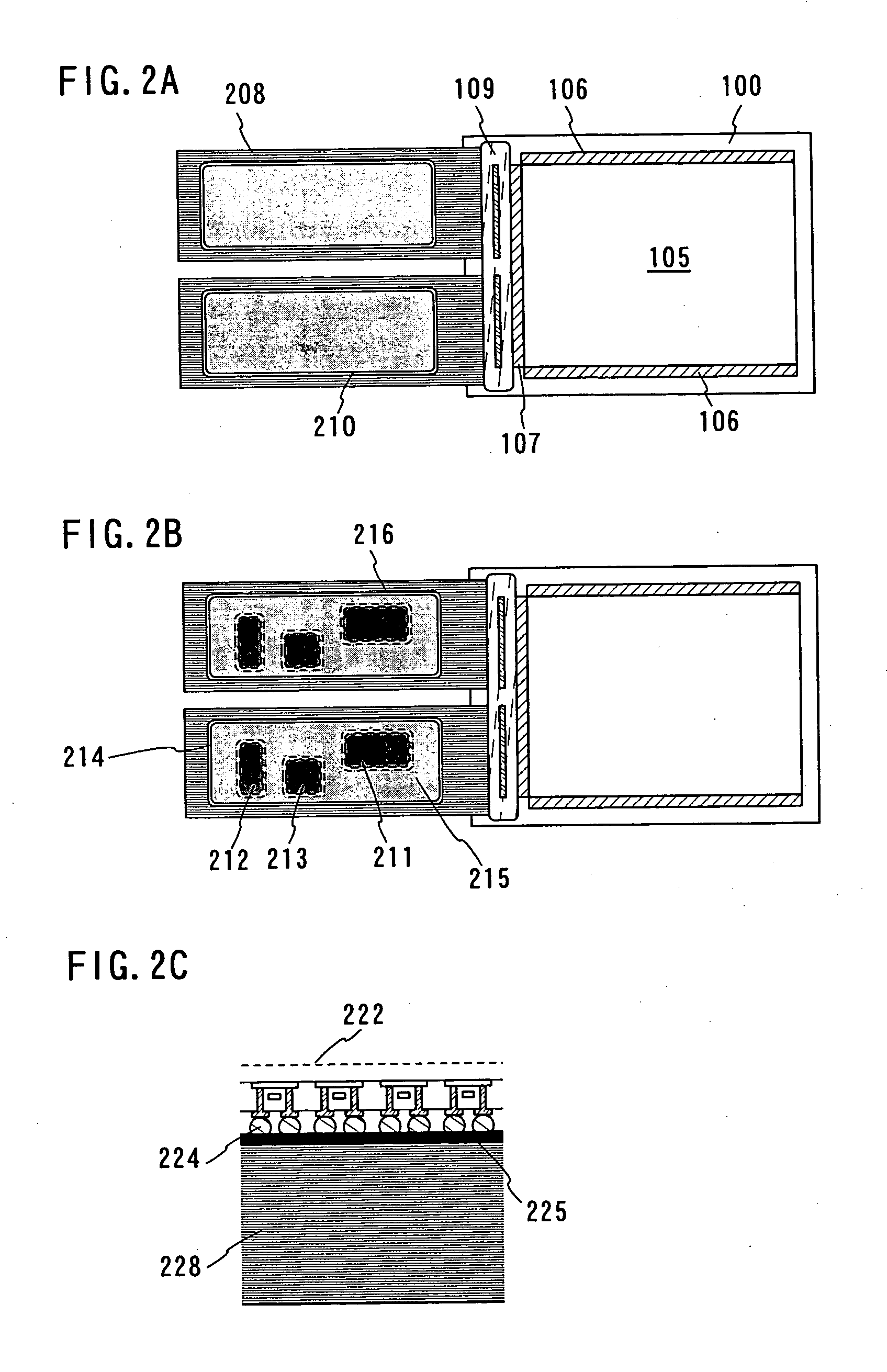
[0054] A module (semiconductor module) in which a driver circuit over a panel is formed by a transfer technique is explained in this embodiment with reference to FIGS. 3A to 3C.

[0055] FIG. 3A is a top view of a semiconductor module. A panel 300 is provided with a pixel portion 305 and a driver circuit (a signal line driver circuit 307, a scanning line driver circuit 306). An FPC (Flexible Printed Circuit) 308 for connecting electrically the driver circuit to an external power source or the like provide at outside (not shown) is pasted onto the panel 300 with an adhesive 309.

[0056] In this embodiment, the driver circuit (the signal line driver circuit 307, the scanning line driver circuit 306) is formed by a transfer technique. Consequently, in case of using a flexible substrate to manufacture a panel, the driver circuit can be formed easily over the flexible substrate.

[0057] FIG. 3B is an enlarged view of the driver circuit (the signal line driver circuit 307, the...

embodiment 3

[0064] Embodiment 3

[0065] In this embodiment, the case that an integrated circuits (a controller 401, a CPU 402, a memory 403) formed over a flexible substrate by a transfer technique is wholly pasted onto a rear surface of a panel will be explained with reference to FIG. 4.

[0066] FIG. 4A is a top view of a semiconductor module. FIG. 4B is a cross-sectional view of the semiconductor module. A panel 400 is provided with a pixel portion 405 and a driver circuit (a signal line driver circuit 407, a scanning line driver circuit 406). An FPC (Flexible Printed Circuit) 408 for connecting electrically the driver circuit to an external power source or the like provided at outside (not shown) is pasted onto the panel 400 with an adhesive 409.

[0067] A rear surface of the panel 400 is pasted with a flexible substrate 412 provided with an integrated circuit (a controller 401, a CPU 402, a memory 403) with an adhesive 413 by the transfer technique (double transfer) as shown in FIG. 4B.

[0068] The...


PUM


Abstract

To provide a thin film device which becomes possible to be formed in the portion which has been considered impossible to be provided with such device by the conventional technique, and to provide a semiconductor device which occupies small space and which has high shock resistance and flexibility, a device formation layer with a thickness of at most 50 mum which was peeled from a substrate by a transfer technique is transferred to another substrate, hence, a thin film device can be formed over various substrates. For instance, a semiconductor device can be formed so as to occupy small space by pasting a thin film device which is transferred to a flexible substrate onto a rear surface of a substrate of a panel, by pasting directly a thin film device onto a rear surface of a substrate of a panel, or by transferring a thin film device to an FPC which is pasted onto a substrate of a panel.

Description

[0001] 1. Field of the Invention[0002] The present invention relates to a transfer technique of manufacturing a device formation layer including a semiconductor device composed of a plurality of thin film transistors (hereinafter, TFT).[0003] 2. Related Art[0004] In recent years, a technique for forming a TFT using a semiconductor thin film (having a thickness of from approximately several to several hundreds nm) formed over a substrate having an insulating surface has been attracted attention. A TFT is utilized widely for an electronic device such as an IC, an electro-optical device, or the like.[0005] As a substrate for forming these TFTs, a glass substrate or a quartz substrate is widely used now, however, these substrates have some drawbacks such as being fragile and heavy. Further, these substrates are unsuitable for mass-production since it is difficult to use a large-sized glass substrate or a large-sized quartz substrate. Therefore it has been attempted that a device compose...

Claims


Application Information

Patent Timeline
IPC IPC(8): H01L31/0392
CPCH01L21/6835H01L27/1214H01L27/1266H01L2221/68368H01L2224/16225H01L2224/32225H01L2224/73204H01L2924/07811H01L2924/00H01L2224/05172H01L2224/05624H01L2924/00014H01L2224/05639H01L2224/05647H01L2224/05664H01L2224/05681H01L2224/05684H01L2224/05124H01L2224/05147H01L2224/05184
Inventor YAMAZAKI, SHUNPEITAKAYAMA, TORUMARUYAMA, JUNYAGOTO, YUUGOOHNO, YUMIKOARAI, YASUYUKISHIBATA, NORIKO
Owner SEMICON ENERGY LAB CO LTD
Why Eureka
Try Eureka