
Multilayer ceramic electronic component and mounting structure and method for the same

Active Publication Date: 2004-12-02
MURATA MFG CO LTD
View PDF3 Cites 57 Cited by
  • Summary
  • Abstract
  • Description
  • Claims
  • Application Information

AI Technical Summary

Problems solved by technology

If, therefore, high voltage is applied on the monolithic ceramic capacitor 1, surface leakage (discharge across the external electrodes 4) readily occurs, which reduces the voltage resistance.
These solder alloys, however, have inferior wettability than conventional Sn-Pb alloys.
Therefore, if the surfaces of the external electrodes 4 are oxidized, the use of these solder alloys may lead to unsuccessful mounting.
The thermoplastic resin layer 22, if having a thickness less than about 1.0 .mu.m, exhibits poor environmental resistance, particularly poor moisture resistance.
Then, the surfaces of the external electrodes 20 lose cleanliness, which deteriorates the wettability of the molten solder and prevents stable solderability.
The thermoplastic resin layer 22, if having a thickness more than about 50 .mu.m, exhibits good environmental resistance but poor flowability in the soldering.
Such poor flowability deteriorates the contact of the molten solder and the external electrodes 20, which obstructs the wetting or causes variations in the start time for the wetting and prevents stable solderability.
Such a thick thermoplastic resin layer 22 also cannot form a normal fillet, which decreases the reliability of the electrical and mechanical connection between the monolithic ceramic capacitor 10 and the substrate 30.
Thus, water penetrates the resins more readily to cause deterioration from inside the resins, leading to low durability.
Such penetrating water also causes difficulty in retaining the cleanliness of the surfaces of the external electrodes 20, and thus, failing to ensure the solderability.
Thus, it cannot provide environmental resistance after mounting.
Such a peeling resin layer also cannot provide voltage resistance if the peeling occurs between the two external electrodes 20.

Method used


Image

  • Multilayer ceramic electronic component and mounting structure and method for the same
  • Multilayer ceramic electronic component and mounting structure and method for the same
  • Multilayer ceramic electronic component and mounting structure and method for the same

Examples


Embodiment Construction

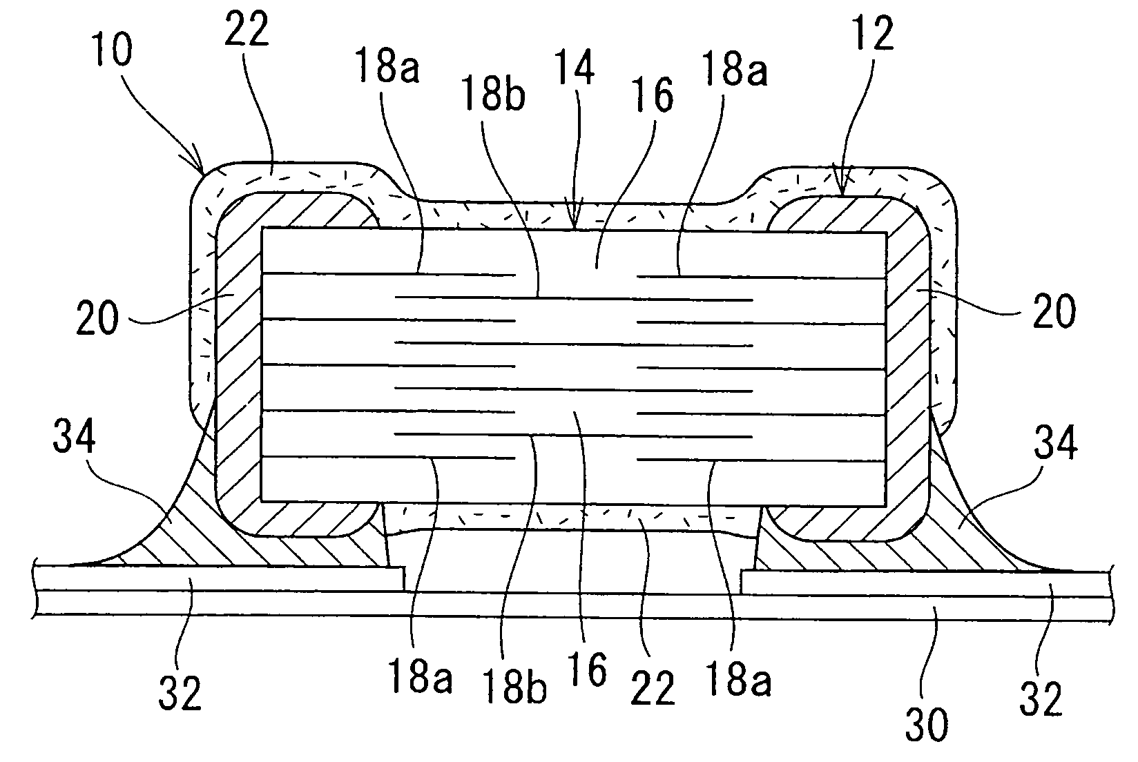
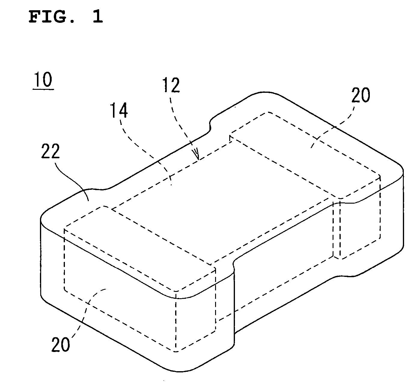
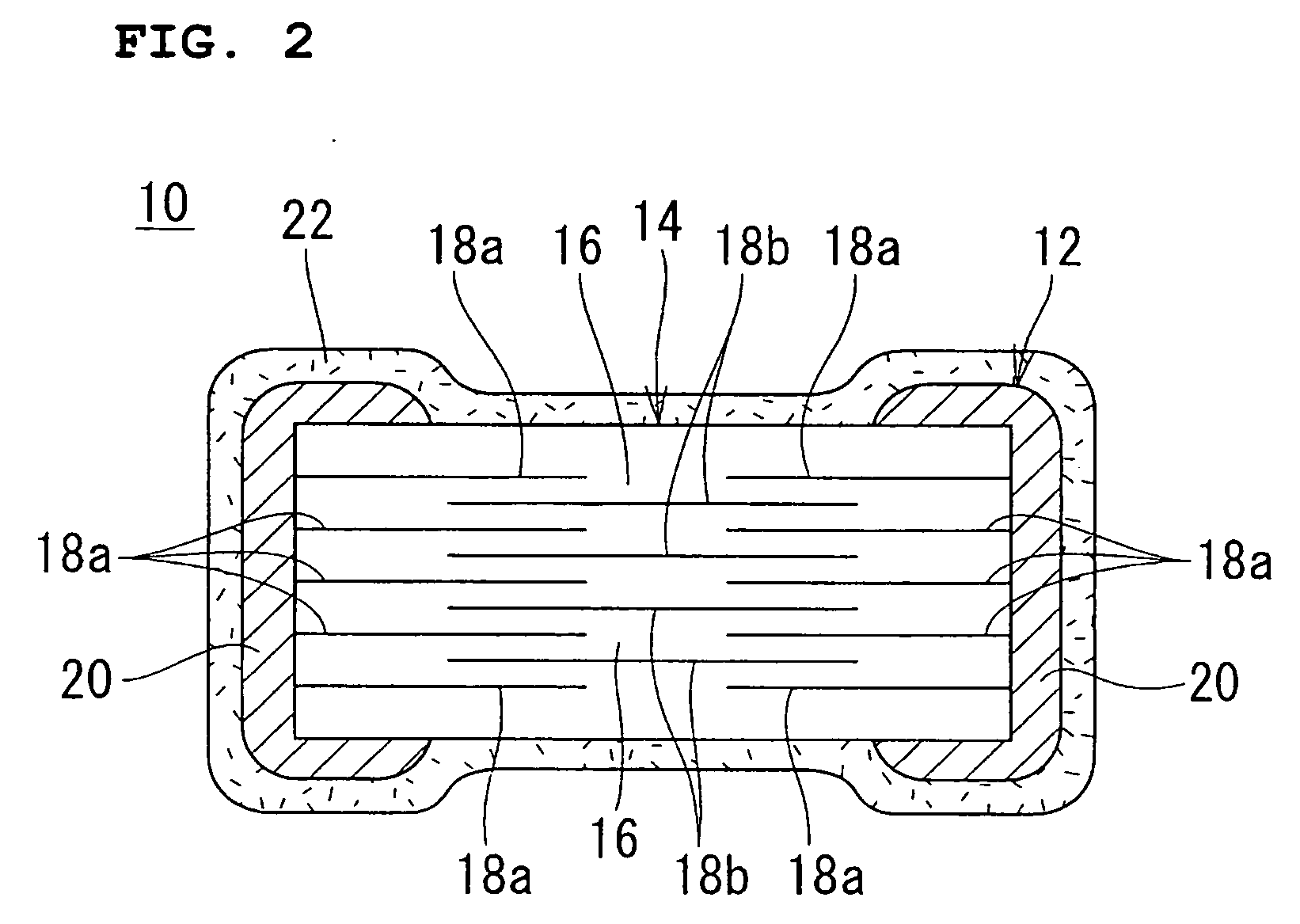
[0047] Monolithic ceramic capacitors were produced as an example of multilayer ceramic electronic components according to various preferred embodiments of the present invention. First, a ceramic slurry was prepared from a dielectric ceramic material. This slurry was shaped with PET films to form ceramic green sheets having a thickness of about 20.0 .mu.m. Then, internal electrode patterns that provide thousands of chips for each printed area were printed on the ceramic green sheets with a nickel paste. The amount of the paste applied was adjusted such that the electrode thickness after firing was about 1.0 .mu.m.

[0048] These ceramic green sheets were dried. Then, a predetermined number of the sheets were laminated, pressed under predetermined conditions, and cut to a predetermined size to form green chips, where the target capacitance was 1,000 pF. These green chips were fired at a predetermined temperature to prepare base composites of ceramic layers and internal electrodes. Subseq...


PUM

PropertyMeasurementUnit
Thicknessaaaaaaaaaa
Electrical conductoraaaaaaaaaa

Abstract

A multilayer ceramic electronic component is prepared by covering a capacitor element with a thermoplastic resin layer that is mounted on a substrate by soldering. The thermoplastic resin layer is molten due to the heat required for soldering. The molten resin layer flows to expose external electrodes of the electronic component. The exposed external electrodes are soldered to electrodes of the substrate. In the resultant mounting structure, the thermoplastic resin layer covers substantially the entire surface except for the soldered portion of the electronic component and a portion of the solder.

Description

[0001] 1. Field of the Invention[0002] The present invention relates to multilayer ceramic electronic components and mounting structures and methods for the electronic components. In particular, the present invention relates to a multilayer ceramic electronic component, such as a monolithic ceramic capacitor, a structure in which the electronic component is mounted on a substrate by soldering, and a method for mounting the electronic component on the substrate by soldering.[0003] 2. Description of the Related Art[0004] A monolithic ceramic capacitor is an example of multilayer ceramic electronic components. Referring to FIG. 5, a monolithic ceramic capacitor 1 includes a base composite of ceramic layers 2 and internal electrodes 3. The internal electrodes 3 are arranged across the thickness of the base composite, are alternately led to either end surface of the base composite, and are connected to external electrodes 4 disposed at both end surfaces of the base composite. The monolit...

Claims


Application Information

Patent Timeline
IPC IPC(8): H01G4/12H01G2/10H01G4/224H05K1/18H05K3/34
CPCH01G2/103H05K3/3442H05K2201/0129Y10T29/43H05K2201/10977Y10T29/435H05K2201/10636Y02P70/50H01G4/12
Inventor KAYATANI, TAKAYUKIKOBAYASHI, SHINICHI
Owner MURATA MFG CO LTD
Features
  • Generate Ideas
  • Intellectual Property
  • Life Sciences
  • Materials
  • Tech Scout
  • Unparalleled Data Quality
  • Higher Quality Content
  • 60% Fewer Hallucinations
Learn More