

Tracking cells for a memory system
a memory system and tracking cell technology, applied in the field of reading memory devices, can solve the problems of limiting the endurance of prior flash memory devices, affecting the performance of flash memory devices, and prone to damag
Inactive Publication Date: 2004-12-16
SANDISK TECH LLC
View PDF59 Cites 529 Cited by
- Summary
- Abstract
- Description
- Claims
- Application Information
AI Technical Summary
Benefits of technology
[0017] These and other objects and advantages of the present invention will appear more clearly from the following description in which the preferred embodiment of the invention has been set forth in conjunction with the drawings.
Problems solved by technology
With use, defects tend to build up in the memory device and may eventually render the device unreliable.
One physical phenomenon limiting the endurance of prior flash memory devices is the trapping of electrons in the active dielectric between the floating gate and the substrate.
If program / erase cycling is continued, the device may eventually experience catastrophic failure.
This problem is even more critical if multi-state memory is implemented, since more accurate placement of the threshold voltage is demanded.
A second problem pertains to charge retention on the floating gate.
For example, negative charge on the floating gate tends to diminish somewhat through leakage over a period of time.
A third problem is that the program / erase cycles may not be performed evenly for the cells in the memory device.
Such uneven programming and erasing causes non-uniform stress conditions for the cells in a particular sector.
Non-uniformity of the program / erase cycling histories can result in a wider distribution of threshold voltages for any particular given state.
In addition to widening the threshold distributions, certain cells may reach closure of the voltage window, device failure or charge retention issues earlier than others.
Polycides are generally not used in place of either the first or second polysilicon layers because the quality of inter-polycrystalline-silicon oxides formed from a polycide is usually not satisfactory.
The voltage gradient across the select gate dielectric can be reduced by making it thicker or selected to have a dielectric constant that is higher than normally used but that can adversely affect operation of the select transistor.
Because of the large threshold voltage delta separating states P1 and P6, it will be highly improbable for a sufficient number of tracking cells to be misdetected (interchanging a higher threshold voltage range for a lower and / or vice versa), without the data portion being massively corrupted as well.
Keeping them at the tail end eliminates a need to shift them out on an ongoing basis, which potentially saves a small amount of time during read but potentially requires shifting out the entire sector of data to read the tracking information when needed.
This also tends to physically bunch up the tracking cells in a localized area of the sector, making it vulnerable to localized variation.
Physically disbursing the tracking cells throughout the sector improves the ability to reflect local variations within a sector, but is cumbersome to manage and use.
If TrackingDone is set to True, then the read process fails.
This error is used to create the quality gauge.
However, greater than one failure would be flagged, since the likelihood of two such random, uncorrelated errors is highly improbable, indicative of a more widespread failing condition existing within the sector.
Nevertheless, given its rare incidence, the overall performance impact is anticipated to be minimal and far preferable to outright read failure or mis-correction.
Method used
View moreImage
Smart ImageViewing Examples

Examples
Embodiment Construction
has been presented for purposes of illustration and description. It is not intended to be exhaustive or to limit the invention to the precise form disclosed. Many modifications and variations are possible in light of the above teaching. The described embodiments were chosen in order to best explain the principles of the invention and its practical application to thereby enable others skilled in the art to best utilize the invention in various embodiments and with various modifications as are suited to the particular use contemplated. It is intended that the scope of the invention be defined by the claims appended hereto.
Login to View More PUM
 Abstract
Tracking cells are used in a memory system to improve the read process. The tracking cells can provide an indication of the quality of the data and can be used as part of a data recovery operation if there is an error. The tracking cells provide a means to adjust the read parameters to optimum levels in order to reflect the current conditions of the memory system. Additionally, some memory systems that use multi-state memory cells will apply rotation data schemes to minimize wear. The rotation scheme can be encoded in the tracking cells based on the states of multiple tracking cells, which is decoded upon reading.
Description
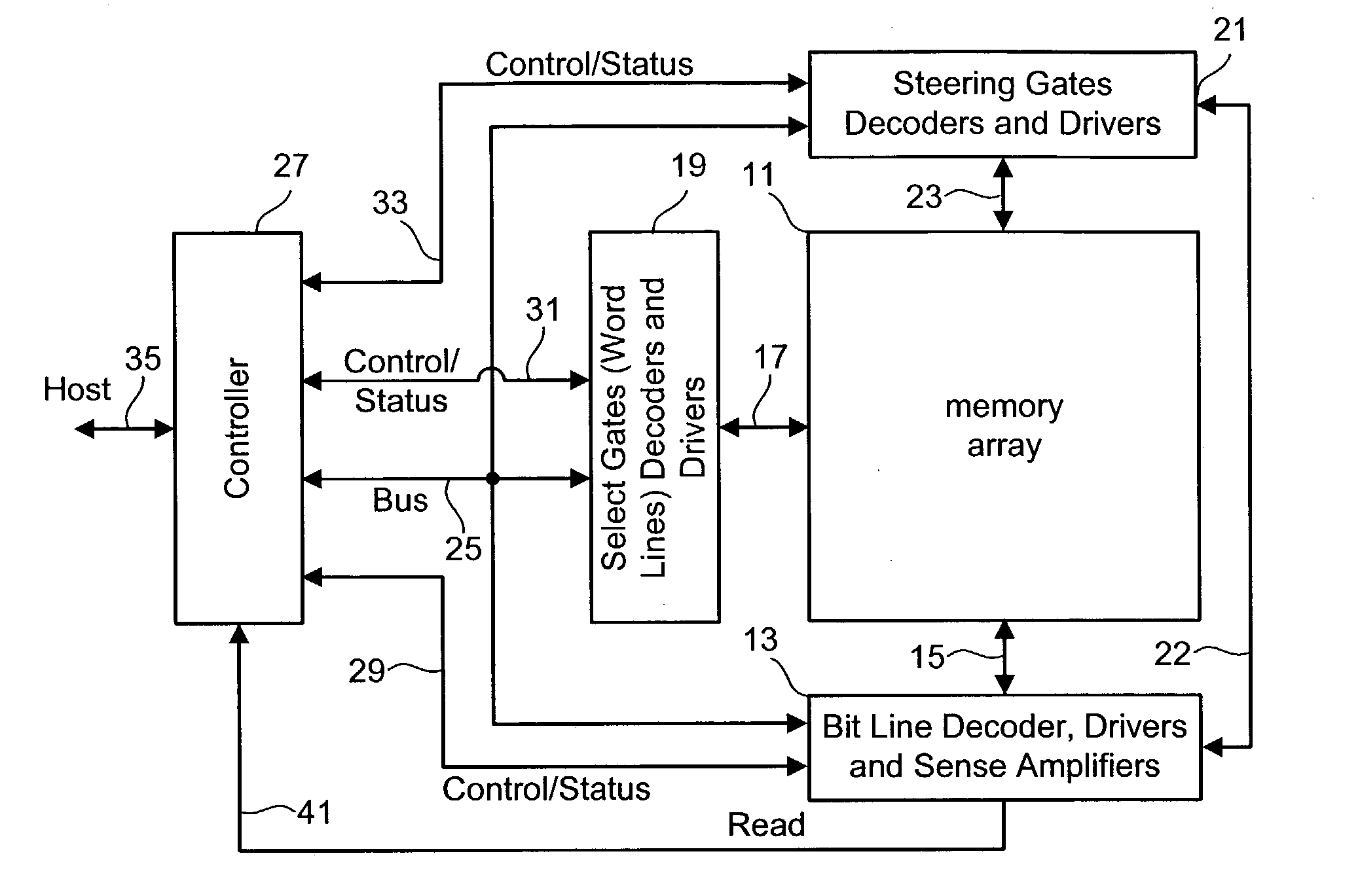
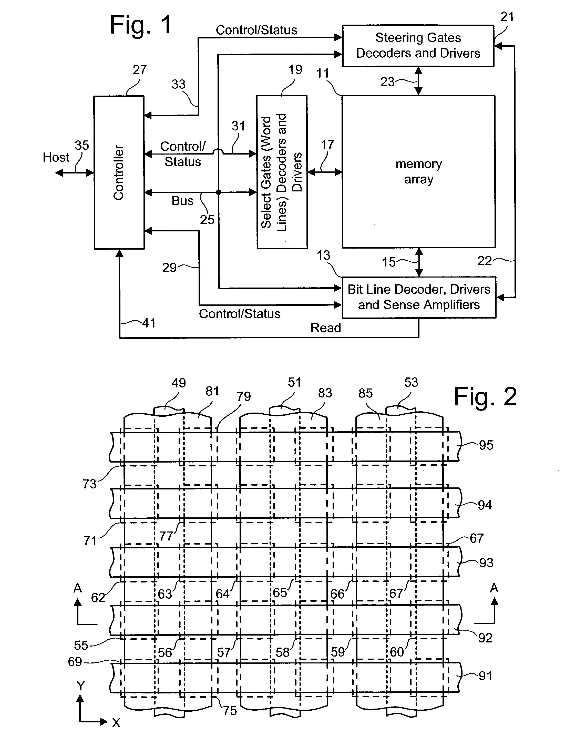
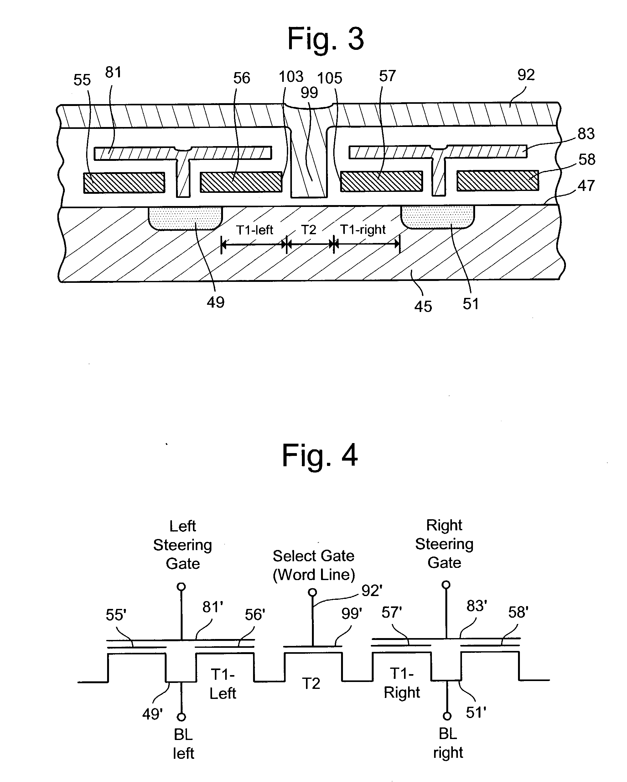
[0001] 1. Field of the Invention[0002] The present invention is directed to technology for reading memory devices.[0003] 2. Description of the Related Art[0004] Semiconductor memory devices have become more popular for use in various electronic devices. For example, non-volatile semiconductor memory is used in cellular telephones, digital cameras, personal digital assistants, mobile computing devices, non-mobile computing devices and other devices. Electrical Erasable Programmable Read Only Memory (EEPROM) and flash memory are among the most popular non-volatile semiconductor memories.[0005] Both EEPROM and flash memory utilize a floating gate that is positioned above and insulated from a channel region in a semiconductor substrate. The floating gate is positioned between source and drain regions. A control gate is provided over and insulated from the floating gate. The threshold voltage of the transistors is controlled by the amount of charge that is retained on the floating gate. ...
Claims
Login to View More Application Information
Patent Timeline
 Patent Type & AuthorityApplications(United States)
IPC IPC(8): G06F12/00G11C11/00G11C11/409G11C11/56G11C16/26G11C16/34
CPCG11C11/5621G11C16/26G11C16/349G11C11/56G11C16/00
InventorGUTERMAN, DANIEL C.GROSS, STEPHEN J.KHALID, SHAHZADGONGWER, GEOFFREY S.
OwnerSANDISK TECH LLC